We are an expert of semiconductor wafers in semiconductor industry, and we offer technology support and wafers selling for thousands of univerisities and industrial customers by our decades experience, including Cornell University, Stanford Univeristy,Peking University, Shandong Univerity, university of south carolina,Caltech Faraon lab (USA),University of California, Irvine (USA),Singapore MIT Alliance for Research and Technology Centre (SMART),West Virginia University,Purdue Univerity, University of California, Los Angeles,King Abdullah University of Science & Technology,Massachusetts Institute of Technology,University of Houston,University of Wisconsin,University of Science and Technology of China etc.
And now we show one article example as follows, who bought our wafers or service:
Article title:Evidence for Deep Acceptor Centers in Plant Photosystem I Crystals
Published by:
Irina Volotsenko ; Michel Molotskii ; Anna Borovikova ; Nathan Nelson ; Yossi Rosenwaks.
Department of Physical Electronics, Faculty of Engineering, and Department of Biochemistry and Molecular Biology, Faculty of Life Sciences, Tel Aviv University, Tel Aviv 69978, Israel.
Picture of SiC wafer:
Abstract
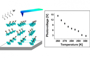
Dry micrometer-thick crystalline photosystem I (PSI) has been shown to generate unprecedented large photovoltage under illumination. We use variable-temperature Kelvin probe force microscopy to show that deep acceptor centers are responsible for this anomalous photovoltage. We assumed that these centers are located close to the positively charged FB2+ clusters, forming a coupled center that effectively captures the photoexcited electron into a deep state. We extract the main inherent parameters of the deep centers, which are extremely important in the potential use of photosynthetic proteins in various optoelectronic devices.
Article abstract for Using Wafer from Xiamen Powerway Advanced Material Co. Ltd. (PAM-XIAMEN) or Powerway Wafer Co.,Limited
“… anomalous PV in the PSI crystals. We have used purified plant PSI crystals (Figure 1c) placed on the cleaned C-face doped SiC substrates (Xiamen Powerway Advanced Materials Co., Ltd.). Figure 2a shows the schematics …”
Source:https://pubs.acs.org/doi/abs/10.1021/jp5112422
About Xiamen Powerway Advanced Material Co., Ltd
PAM-XIAMEN offers semiconductor silicon carbide wafers,6H SiC and 4H SiC wafer in different quality grades for researcher and industry manufacturers. We has developed SiC crystal growth technology and SiC wafer processing technology. We provide custom thin film (silicon carbide)SiC epitaxy on 6H or 4H substrates for the development of silicon carbide devices. SiC epi wafer is mainly used for Schottky diodes, metal-oxide semiconductor field-effect transistors, junction field effect.
PAM-XIAMEN also offer GaAs/InP and GaN material from wafer substrate to epitaxial growth.
Powerway Wafer Co.,Limited is a sub company of Xiamen Powerway Advanced Material Co., Ltd specialize in dealing with overseas orders.
Are You Looking for an Semiconductor wafer?
PAM-XIAMEN is proud to offer semiconductor wafer inlcuidng SiC/GaN/GaAs/InP wafer with wafer or epitaxial wafer for all different kinds of projects. If you are looking for semiconductor wafer, send us enquiry today to learn more about how we can work with you to get you the substrate wafers you need for your next project. Our group team is looking forward to providing both quality products and excellent service for you! For more information, please visit our website:www.powerwaywafer.com, send us email at tech@powerwaywafer.com or powerwaymaterial@gmail.com.