Towards the cost effective epitaxy of hillocks free CdZnTe film on (001)GaAs by close-spaced sublimation
Cost-effective epitaxy of hillocks free CdZnTe films on (001)GaAs was explored with close-spaced sublimation (CSS) technique. The orientation and film quality were studied with scanning electron microscopy (SEM), X-ray diffraction θ–2θ and Φ scans and rocking, and cross-sectional transmission electron microscopy (TEM). It is found that higher deposition rate and better film quality can be achieved simultaneously at the elevated source and substrate temperatures. The full width half maximum (FWHM) of the X-ray rocking curve for (004) plane of the best CdZnTe film obtained so far is 306 arcsec, which was deposited at a rate of 1 μm/min under 100 Pa of Ar. The hillocks are believed to be prevented due to the prevention of the formation and propagation of long stacking faults.
Highlights
► Hillocks free CdZnTe epi-layer was grown by a one-step CSS process.
► Higher growth rate and better film quality can be achieved simultaneously.
► The FWHM of (004) rocking curve of the film deposited at 1 μm/min is 306 arcsec.

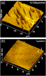
Fig. 1. The AFM images of CdZnTe films deposited under different source and substrate temperature conditions. (a) Condition I, 788 K and 763 K, (b) condition II, 873 K and 848 K.
Source: Materials Letters
If you need more information about Towards the cost effective epitaxy of hillocks free CdZnTe film on (001)GaAs by close-spaced sublimation
,please visit our website:https://www.powerwaywafer.com/, send us email at sales@powerwaywafer.com or powerwaymaterial@gmail.com.