GaN-based light-emitting diode (LED) solid-state lighting has become the most important lighting technology in recent years because it has many advantages such as high conversion efficiency, long life, and eco-friendliness. Due to the lack of natural GaN substrates, GaN-based LED structures are usually fabricated on (0001) c-plane sapphire substrates. The threading dislocations (TDs) will be caused by interface energy difference, which is formed by the mismatch of the lattice constant and thermal expansion coefficient between the sapphire substrate. The dense non-radiative recombination center caused by TD seriously reduces the quantum efficiency of the light-emitting device. Usually, V-shaped pits (V pits), which are have open hexagons, inverted pyramids, and (10-11) faceted sidewalls, can be observed in InGaN/GaN multiple quantum wells (MQWs) along the TDs.
1. What Are V-Shaped Pits in LED Wafer Cross Section?
After successfully etched some test patterns in our GaN LED wafers, we took some SEM images of mesa cross-sections. However, we spotted an unusual shape in some of the images as follows:
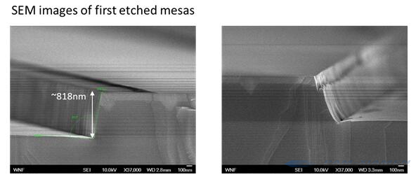
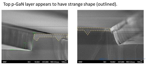
Have you seen anything like this before? Do you have any idea what it might be?
Actually, it is quite normal that all the GaN LED wafers will generate it during the growth of LED epitaxy, which is called v-pit (V shaped pits) or V defect. Only in this way can the LED structure emit light. And the V pits are filled with p-GaN layer.
Details about the V-shape pits please visit: Formation of V-Shaped Pits in Nitride Films Grown by Metalorganic Chemical Vapor Deposition
2. Influences of V Pit in GaN LED Wafer
Previous researches claimed that the pre-strained layer or superlattice (SLS) under the MQW embedded in the LED structure can relax the strain in the layer. But more SLS pairs will accumulate strain energy. Then, partial strain relaxation will lead to the formation of V pits. V-pit size is optimized at about 200-250nm and the opening angle is 60°. Some reports indicate that the V-shaped pits can play a positive role in InGaN-based LEDs, such as inhibiting non-radiative recombination and helping to improve luminous efficiency.
Some scientists have improved the electrical and optical properties by carefully controlling and designing interface strain energy and dislocations, thereby increasing the efficiency of InGaN-based blue LEDs. The use of high-angle circular dark-field scanning transmission electron microscopy and atom probe tomography confirmed the existence of thin quantum wells in the inclined region of the V pit, whose thickness and In concentration are much lower than those of the flat region. It indicates that the thread dislocations in the V-shaped pits act as an energy barrier for the lateral transfer of charges. The influence of the V pit and the energy barrier derived from the (1011) plane is discussed. The higher V pit energy barrier height in InGaN QW can effectively suppress the non-radiant recombination at the TDs, thereby enhancing the internal quantum efficiency (IQE). The superlattice layer is used to operate the nano-level V pits and obtain the best V pit size to achieve high-efficiency blue wavelength InGaN/GaN LEDs.
For more information, please contact us email at victorchan@powerwaywafer.com and powerwaymaterial@gmail.com.