Indium Arsenide (InAs) wafer can be provided by PAM-XIAMEN with a diameter up to 2 inch and a wide choice in off or exact orientation, high or low concentration and surface processed to optoelectronics industry. InAs wafer is an important III-V narrow band gap semiconductor. It has the characteristics of high electron mobility, low effective mass and strong spin-orbit coupling. Therefore, it’s ideal for preparing high-speed and low-power electronic devices, infrared optoelectronic devices and spintronic device, such as synchronization of IR and visible pulses in pump-probe setup. More sepcs of indium arsenide wafer please see the followings:
1. Specifications of Indium Arsenide Substrates
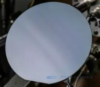
PAM200119-INAS
2-inch indium arsenide wafers with following specifications:
1) Thickness (um): 500;
Orientation: (001);
Type: N;
Dopant: Stannum or S;
Carrier concentration: (5-20) x 1017 cm-3;
Surface preparation: Polished/Polished;
Epi-Ready
2) Thickness (um): 500;
Orientation: (001);
Type: N;
Dopant: Undoped;
Carrier concentration: (1-6) x 1016 cm-3;
Surface preparation: Polished/Polished;
Epi-Ready
2. Defects in the Growth of Indium Arsenide Wafer
It is possible to grow InAsSb/InAsPSb, InNAsSb, AlGaSb and other heterojunction superlattice structure materials on InAs single crystal as substrate to produce infrared light-emitting devices and quantum cascade lasers with wavelengths of 2-14nm. With the continuous improvement of device performance and the reduction of device size, the requirements for junction quality and surface quality of single crystal InAs substrate are getting higher and higher. This requires the study of bulk indium arsenide single crystal growth and wafer polishing, cleaning and other process technologies to reduce and control the defect density in the crystal, avoiding surface damage during the polishing process, and reducing the concentration of residual impurities. However, III-V compound wafer materials are affected by thermal stress and deviation of chemical ratio during the growth process, and are prone to impurity deposition, dislocation clusters, small-angle grain boundaries and other defects. The chemical properties of the indium mono arsenide are unstable, and the material is soft and brittle. Therefore, it is easy to produce processing damage. Studying the causes of these defects will help to improve the high purity indium arsenide wafer growth technology, reduce the defect concentration, and improve the quality and the surface of the indium arsenide thin film.
3. Solutions for Producing High-quality InAs Wafer
A solution is suggested that use the LEC method to grow indium arsenide (100) single crystal. By adjusting the thermal field conditions, keeping the longitudinal temperature gradient below 120K/cm, the InAs ingot is slightly dissociated, and there is only a small amount of adhered B203 on the surface, which fully reduces the crystal thermal stress. In addition, it is necessary to control and standardize the angle of shoulder placement and closing, and the cooling rate, avoiding large temperature fluctuations during the growth process, which will cause thermal shock to affect the crystal. Under such growth conditions, an InAs single crystal with good crystalline quality is obtained. The lattice integrity of the InAs single crystal is quite good. The crystal quality of InAs single crystals grown under As-rich conditions is obviously poor, and such a single crystal indium arsenide wafer is easily broken during processing. Therefore, maintaining a rich indium condition is conducive to obtaining high-quality InAs single crystal with good performance, low dislocation density, and no clusters and linear dislocations.

For more information, please contact us email at victorchan@powerwaywafer.com and powerwaymaterial@gmail.com.