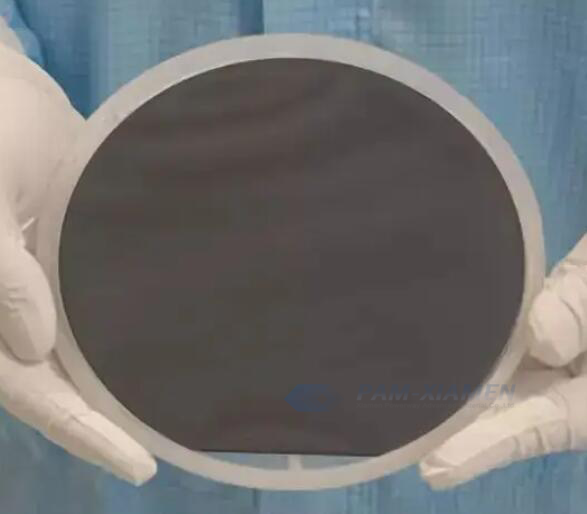
Quaternary direct bandgap compound materials, such as InGaAsP and AlGaInAs, can be grown on InP substrate, which are lattice match with InP. At present, in various fields, researchers have designed semiconductor lasers, optical amplifiers, detectors, etc., using these two types of materials grow on InP substrate. For optical amplifiers, high power 1460nm semiconductor laser based on AlGaInAs / InP MQW is an ideal pump source. PAM-XIAMEN can grow 1460nm AlGaInAs / InP pump laser diode epitaxial wafer for optical amplification. The exact pump laser epi structure please refer to the table below:
1. 1460nm Pump Laser Diode Epitaxy Structure
PAM230509 – 1460LD
| Layer No. | Material | Thickness(nm) | Dopant | Type |
| 6 | InP | – | – | – |
| 5 | GaIn(x)As | – | – | – |
| 4 | GaIn(x)As(y)P | – | – | – |
| 3 | InP | 2100 | – | – |
| 2 | AlGaInAs MQW + SCH
PL 1430~1460nm |
– | – | – |
| 1 | InP buffer | – | Silicon | N |
| InP substrate |
For quantum well structures with lasing wavelengths ranging from 1300 to 1700 nm, we usually epitaxy pump laser diode wafer based on InP substrate, and use InGaAlAs material as quantum well. By adjusting the AlGaInAs composition and selecting appropriate quantum well thickness, we can freely design the diode pump laser wavelength over a large range. From Fig. 1, it can be seen that the adjustable corresponding wavelength of AlGaInAs / InP material system for Raman pump laser can be from 1.3 μm to 1.5 μm.
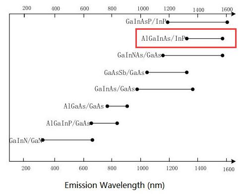
Fig. 1 Wavelength Range Corresponding to AlGaInAs / InP Material
2. Challenges for AlGaInAs Material Growth on InP
The difficulty of epitaxial growth of AlGaInAs mainly includes:
1) The Al component is easily oxidized and forms deep energy levels with O;
2) At the Al (Ga) InAs / InP interface, As and P interdiffusion is prone to occur, affecting the quality of the epitaxial layer. By increasing the temperature and V/II ratio, high-quality Al containing materials can be obtained. However, high temperatures are detrimental to the growth of In containing materials. At high temperatures, the pre-reaction of In and the desorption of the growth surface are more severe, which easily leads to the formation of In droplet distribution on the surface, affecting the luminescent efficiency of the material. Moreover, the higher the growth temperature, the more severe the As and P interdiffusion problem at the interface between AlGaInAs and InP, which affects the uniformity and flatness of the interface. Therefore, the growth temperature range of high-quality AIGalnAs materials is very limited and requires precise control.
3. Optimizing the Energy Band Structure of AlGalnAs / InP Quantum Well Laser
In order to further improve the temperature characteristics of pump laser fiber amplifier devices and enhance the limiting ability of carriers on both sides of the active region of the laser, the energy band structure of AIGalnAs / InP strain quantum well lasers has been optimized in recent years. To summarize briefly:
1) The electron barrier layer (ESL) is introduced into the graded index waveguide layer or the limiting layer to prevent electrons from leaking into the limiting layer. The characteristic temperature and Slope efficiency of pump laser diode can be improved by adding p-AllnAs electron barrier layer between MQW and p-SCH layers;
2) Introduce InP on the N-side of the active region to improve the confinement ability of holes on the N-side;
3) Introducing AllInAs/AlGalnAs multiple quantum barriers (MQBs) in the confinement layer to enhance the confinement ability of charge carriers.

For more information, please contact us email at victorchan@powerwaywafer.com and powerwaymaterial@gmail.com.