For single photon detection technology, in addition to the traditional InP/InGaAs SPAD, new material systems such as low noise material systems constructed from Sb based digital alloys, multi multiplication InP/InGaAs SPAD using ionization engineering, and InAlAs/InGaAs SPAD have also been developed. PAM-XIAMEN can provide InP based InGaAs / InAlAs epitaxial wafer for single photon detector, with the specific structure as follows:
1. MOCVD Grown InP based Heteroepitaxial Wafers for Single Photon Detector
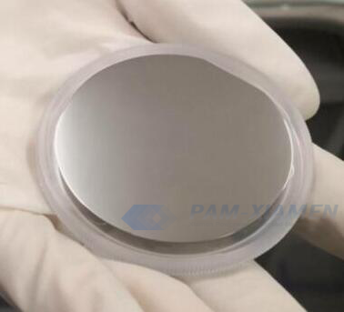
PAM210918 – SPDE
No.1 2inch SPD Heteroepitaxial Wafer
| Layer No. | Material | Thickness (nm) | Dopant | Doping Level (cm-3) |
| 8 | InxGa1-xAs | – | – | – |
| 7 | In0.52Al0.48As | – | – | – |
| 6 | InxGa1-xAs | 50±3 | – | – |
| 5 | InP | – | – | – |
| 4 | InP | – | – | 6*1016±0.3*1016 |
| 3 | InGaAlAs (gradient in chemical composition from InxGa1-xAs to InP: >3 steps) | – | – | – |
| 2 | InxGa1-xAs | – | Si | – |
| 1 | InP | – | – | – |
| 0 | InP Substrate | 350±25um | S | – |
No.2 3inch InP based Epi-Structure for SPD
| Layer No. | Material | Thickness (nm) | Dopant | Doping Level (cm-3) |
| 8 | InxGa1-xAs | – | – | 1.5*1019±0.1*1019 |
| 7 | In0.52Al0.48As | – | – | – |
| 6 | InAlGaAs (numeric gradient in chemical composition from InxGa1-xAs to In0.52Al0.48As: > 13 steps) | – | – | – |
| 5 | InxGa1-xAs | 1700±50 | – | – |
| 4 | InAlGaAs (numeric gradient in chemical composition from In0.52Al0.48As to InxGa1-xAs: > 13 steps) | – | – | – |
| 3 | In0.52Al0.48As | – | C | – |
| 2 | In0.52Al0.48As | – | – | – |
| 1 | In0.52Al0.48As | – | – | – |
| 0 | InP Substrate | 625±25um | S | – |
No.3 3inch InP Epitaxial Structure for SPD
| Layer No. | Material | Thickness (nm) | Dopant | Doping Level (cm-3) |
| 9 | InxGa1-xAs | 50±3 | – | 1.5*1019±0.1*1019 |
| 8 | In0.52Al0.48As | – | – | – |
| 7 | InAlGaAs (numeric gradient in chemical composition from InxGa1-xAs to In0.52Al0.48As: > 13 steps) | – | – | – |
| 6 | InxGa1-xAs | – | – | – |
| 5 | InAlGaAs (numeric gradient in chemical composition from In0.52Al0.48As to InxGa1-xAs: > 13 steps) | – | – | – |
| 4 | In0.52Al0.48As | – | C | – |
| 3 | In0.52Al0.48As | – | – | – |
| 2 | In0.52Al0.48As | – | – | – |
| 1 | InxGa1-xAs | – | – | – |
| 0 | InP Substrate | 625±25um | Semi-insulated | – |
2. What Is A Single Photon Detector?
Single-photon detector relies on its ultra-high sensitivity to detect and count individual photons, and its main function is to convert optical signals into electrical signals. The single photon detector working principle is mainly based on the photoelectric effect. The photoelectric effect is that the change of state occurs after the photons act on the detector, and the photons are measured by measuring changes in electronic states.
Currently, the commonly used SPDs mainly include Photomultiplier tube (PMT), Avalanche photodiode (APD) and superconducting nanowire single photon detector (SNSPD). Among them, PMT and APD are photoelectric devices of traditional single photon technology. In recent years, with the development of optoelectronic detection technology and new structures, various novel optoelectronic detectors have emerged, including quantum dot based single photon detectors, visible photon counters, frequency up conversion based single photon detectors, and superconducting single photon detectors.
3. InP-based Single Photon Detector Applications
Single photon detectors can detect extremely weak light signals and have high sensitivity. In many optical fields, single photon detection techniques are crucial and widely used in various fields:
1) Quantum communication: In the field of quantum communication, single photons are used as quantum superposition state encoding and transmission carriers, thus single photon detectors are widely used as the core detection devices of quantum communication systems;
2) Single photon laser ranging: In the field of laser ranging, a narrow pulse laser sequence is emitted from a target, and distance information can be obtained by recording the flight time of the light signal back and forth to the target under known light speed conditions;
3) InP based SPD can be made into single photo detector array applied in fields such as laser 3D imaging, 3D terrain mapping, autonomous navigation for unmanned vehicles, and passive imaging in sparse photon environments.

For more information, please contact us email at victorchan@powerwaywafer.com and powerwaymaterial@gmail.com.