PAM XIAMEN offers 12″ Silicon Wafer.
Material
Orient.
Diam.
Thck
(μm)
Surf.
Resistivity
Ωcm
Comment
p-type Si:B
[100]
12″
750
P/E
MCZ 1-100
TEST grade, SEMI notch, TTV<25µm
p-type Si:B
[100]
12″
775
P/P
MCZ 1-100
Prime, SEMI notch, TTV<3µm
p-type Si:B
[100]
12″
775
P/E
MCZ 1-100
Prime, SEMI notch,TTV<10µm
p-type Si:B
[100]
12″
775
P/P
0.01-0.02
Prime, SEMI notch,TTV<4µm
For more information, please visit our website: https://www.powerwaywafer.com,
send us email at sales@powerwaywafer.com and powerwaymaterial@gmail.com
Found in 1990, Xiamen Powerway Advanced Material Co., Ltd (PAM-XIAMEN) is a leading [...]
2019-03-04meta-author
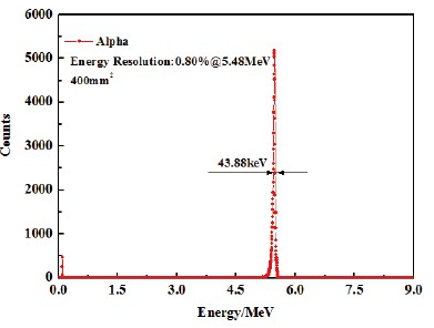
Low Temperature GaAs Test Report
https://www.powerwaywafer.com/low-temperature-gaas-2.html
For more information, please visit our website: https://www.powerwaywafer.com,
send us email at sales@powerwaywafer.com and powerwaymaterial@gmail.com
Found in 1990, Xiamen Powerway Advanced Material Co., Ltd (PAM-XIAMEN) is a leading manufacturer of semiconductor material in China. PAM-XIAMEN develops advanced crystal growth and epitaxy technologies, manufacturing [...]
2019-03-20meta-author
PAM-XIAMEN can supply GaN wafers for LD, LED, HEMT and other applications. You can click following links for more GaN wafer specifications:
GaN based LED epitaxial wafer: https://www.powerwaywafer.com/gan-wafer/epitaxial-wafer.html;
GaN HEMT epitaxial wafer: https://www.powerwaywafer.com/gan-wafer/gan-hemt-epitaxial-wafer.html;
Blue GaN LD wafer: https://www.powerwaywafer.com/blue-gan-ld-wafer.html.
Why you need to choose GaN wafers for power devices?
The short video: https://youtu.be/5Uk9HVzQWAc [...]
2022-09-26meta-author
Semiconductor sensor refers to a sensor made by utilizing various physical, chemical, and biological characteristics of semiconductor materials. The majority of the semiconductor materials used are silicon, as well as III-V and II-VI element compounds. The researchers used the excellent performance and availability of SiC [...]
2023-11-03meta-author
PAM XIAMEN offers SiO2 (single crystal quartz).
Single crystal quartz wafer is an excellent substrate for microwave filters for wireless communication industries.
Conversion from the three-index system to the four as [u ‘ v ‘ w ‘ ] —> [u v t w] is [...]
2019-05-15meta-author
PAM XIAMEN offers 6″ Silicon Wafer.
Material
Orient.
Diam.
Thck
(μm)
Surf.
Resistivity
Ωcm
Comment
p-type Si:B
[100]
6″
675
P/E
1-100
SEMI Prime, 1Flat (57.5mm)
p-type Si:B
[100]
6″
800
E/E
1-50
SEMI, 1Flat (57.5mm), TTV<5μm
p-type Si:B
[100]
6″
320
P/E
0.001-0.030
JEIDA Prime
p-type Si:B
[100]
6″
675
P/P
0.001-0.005
SEMI Prime, 1Flat (57.5mm)
p-type Si:B
[100]
6″
675
P/E
0.001-0.005
SEMI Prime, 1Flat (57.5mm)
p-type Si:B
[111-4.0°] ±0.5°
6″
625
P/E
4-15 {7.1-8.8}
SEMI Prime, 1 JEIDA Flat(47.5mm)
p-type Si:B
[111] ±0.5°
6″
675
E/E
0.010-0.025
SEMI, 1Flat (57.5mm)
n-type Si:P
[100]
6″
925 ±15
E/E
5-35 {12.5-29.7}
JEIDA Prime, TTV<5μm
n-type Si:P
[100]
6″
675
P/E
2.7-4.0
SEMI Prime
n-type Si:P
[100]
6″
250 ±5
P/P
1-3
SEMI [...]
2019-03-04meta-author