PAM XIAMEN offers silicon wafers
Silicon Wafer Mobility Calculator
Indium Tim Oxide (ITO) – Float Zone Silicon – LiNbO3 – InGaAs – Nitride on Silicon – Aluminum – Silicon Carbide (SiC) – GaN on Sapphire
For more information, please visit our website: https://www.powerwaywafer.com,
send us email at sales@powerwaywafer.com and powerwaymaterial@gmail.com
Found in 1990, Xiamen Powerway Advanced Material Co., Ltd (PAM-XIAMEN) is a [...]
2019-02-25meta-author
Highlights
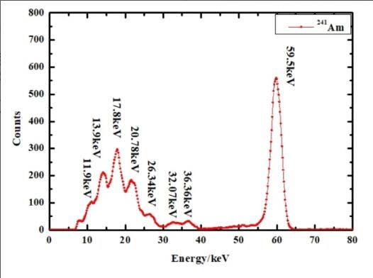
•The thickness of graphene grown on SiC was determined by AES depth profiling.
•The AES depth profiling verified the presence of buffer layer on SiC.
•The presence of unsaturated Si bonds in the buffer layer has been shown.
•Using multipoint analysis thickness distribution of the graphene on [...]
As reported by Esia(European Semiconductor Industry Association), in January worldwide sales of semiconductors amounted to US$ 26.880 billion. These results are in line with seasonal patterns – as the first months of the year are usually slower for semiconductors – and represent a 2.7% [...]
2016-04-18meta-author
PAM-XIAMEN offers A Plane Si-GaN Freestanding GaN Substrate
Item
PAM-FS-GAN A-SI
Dimension
5 x 10 mm2 or 5 x 20 mm2
Thickness
380+/-50um
Orientation
A plane (11-20) off angle toward M-axis 0 ±0.5°
A plane (11-20) off angle toward C-axis -1 ±0.2°
Conduction Type
Semi-Insulating
Resistivity (300K)
> 10 6Ω·cm
TTV
≤ 10 µm
BOW
BOW ≤ 10 µm
Surface Roughness:
Front side: Ra<0.2nm, epi-ready;
Back side: Fine Ground or polished.
Dislocation Density
≤ 5 x 106 cm-2
Macro Defect Density
0 cm-2
Useable Area
> 90% (edge exclusion)
Package
each in single wafer container, under nitrogen atmosphere, packed in class 100 clean room
For more information, please contact us email at victorchan@powerwaywafer.com and powerwaymaterial@gmail.com
2020-08-17meta-author
PAM XIAMEN offers 4″ Silicon Wafer.
Material
Orient.
Diam.
Thck
(μm)
Surf.
Resistivity
Ωcm
Comment
n-type Si:P
[100]
4″
525
P/E
FZ 4,200-8,000
SEMI TEST (Bad Surface & Chips), Lifetime>1,400μs, in Empak cassettes of 7 & 7 wafers
n-type Si:P
[100] ±0.2°
4″
380 ±10
P/E
FZ >3,500
SEMI TEST , 1 Flat
n-type Si:P
[100]
4″
400 ±10
P/P
FZ 3,100-6,800
SEMI Prime, TTV<5μm
n-type Si:P
[100]
4″
200
P/P
FZ >3,000
SEMI Prime, MCC Lifetime > 1,000μs,
n-type Si:P
[100]
4″
400
P/E
FZ 2,000-6,500
SEMI Prime, Lifetime>1,000μs
n-type Si:P
[100]
4″
915 ±10
E/E
FZ 2,000-3,000
1Flat at [100]
n-type Si:P
[100]
4″
300
L/L
FZ 1,100-1,600
SEMI
n-type Si:P
[100] ±1°
4″
200 [...]
2019-03-05meta-author
PAM XIAMEN offers prime grade silicon wafers for research and production. We have ultra-thin silicon 5 micron thin to silicon wafer pucks 10mm thick. All orientation and resistivities, both highly doped and low doped specifications.
What are Silicon Wafer Grades?
Silicon wafers are available in different [...]
2019-02-25meta-author