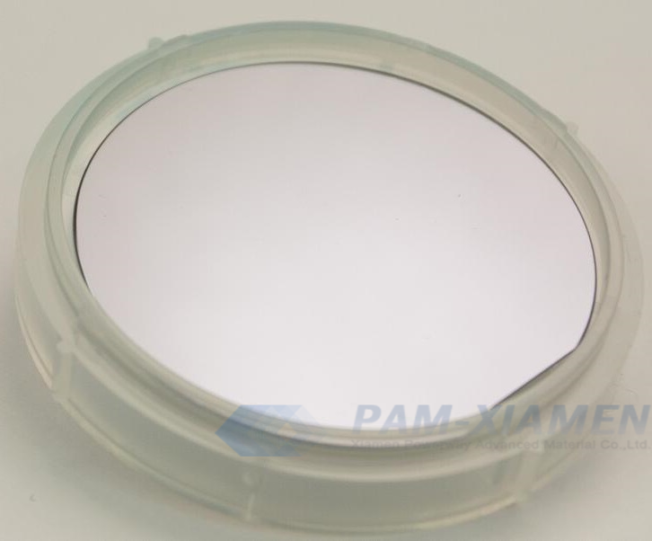
Indium phosphide (InP) is one of the III-V compound semiconductors. It is a new generation of electronic functional materials after silicon and gallium arsenide. Indium phosphide semiconductor material has many excellent properties: direct transition band structure, high photoelectric conversion efficiency, high electron mobility, easy to make semi insulating materials, suitable for making high-frequency microwave devices and circuits, high working temperature (400-500 ℃) and so on. These advantages make indium phosphide wafers widely used in solid state luminescence, microwave communications, optical communications, satellites and other fields. PAM-XIAMEN is able to offer conductive indium phosphide semiconductor wafer. More additional wafer information, please view: https://www.powerwaywafer.com/compound-semiconductor/inp-wafer.html.
The P-type indium phosphide substrates, which are mainly prepared by Zn doping, are listed as follows for your reference:
1. Indium Phosphide Semiconductor Substrate Parameters
No. 1 50.5mm InP Substrate
| Item | Parameter | UOM | |||
| Material | InP | ||||
| Conduction Type/Dopant | S-C-P/Zn | ||||
| Grade | Prime | ||||
| Diameter | 50.5±0.4 | mm | |||
| Orientation | (100)±0.5° | ||||
| Orientation Angle | / | ||||
| Flat Option | EJ | ||||
| Primary Flat Orientation | (0-1-1)±0.02° | ||||
| Primary Flat Length | 16±1 | ||||
| Secondary Flat Orientation | (0-11) | ||||
| Secondary Flat Length | 7±1 | mm | |||
| Carrier Concentration | Min | 0.6E18 | Max | 6E18 | cm-3 |
| Resistivity | Min | / | Max | / | ohm*cm |
| Mobility | Min | / | Max | / | cm2/V*sec |
| EPD | Ave | <1000 | Max | / | cm-2 |
| Laser Mark | Back side major flat | ||||
| Edge Rounding | 0.25 (conform to SEMI Standards) | mmR | |||
| Thickness | Min | 325 | Max | 375 | μm |
| TTV | Max | 10 | μm | ||
| TIR | Max | 10 | μm | ||
| BOW | Max | 10 | μm | ||
| Warp | Max | 15 | μm | ||
| Surface | Side 1 | Polished | Side 2 | Etched | |
| Particle Count | / | ||||
| Package | Individual container filled with N2 | ||||
| Epi-ready | Yes | ||||
| Remark | Special specifications will be discussed separately | ||||
No.2 76.2mm InP Wafer
| Item | Parameter | UOM | |||
| Material | InP | ||||
| Conduction Type/Dopant | S-C-P/Zn | ||||
| Grade | Prime | ||||
| Diameter | 76.2±0.4 | mm | |||
| Orientation | (100)±0.5° | ||||
| Orientation Angle | / | ||||
| Flat Option | EJ | ||||
| Primary Flat Orientation | (0-1-1) | ||||
| Primary Flat Length | 22±1 | ||||
| Secondary Flat Orientation | (0-11) | ||||
| Secondary Flat Length | 12±1 | mm | |||
| Carrier Concentration | Min | 0.6E18 | Max | 6E18 | cm-3 |
| Resistivity | Min | / | Max | / | ohm*cm |
| Mobility | Min | / | Max | / | cm2/V*sec |
| EPD | Ave | <1000 | Max | / | cm-2 |
| Laser Mark | Back side major flat | ||||
| Edge Rounding | 0.25 (conform to SEMI Standards) | mmR | |||
| Thickness | Min | 600 | Max | 650 | μm |
| TTV | Max | 10 | μm | ||
| TIR | Max | 10 | μm | ||
| BOW | Max | 10 | μm | ||
| Warp | Max | 15 | μm | ||
| Surface | Side 1 | Polished | Side 2 | Etched | |
| Particle Count | / | ||||
| Package | Individual container filled with N2 | ||||
| Epi-ready | Yes | ||||
| Remark | Special specifications will be discussed separately | ||||
No.3 100mm InP Semiconductor Wafer
| Item | Parameter | UOM | |||
| Material | InP | ||||
| Conduction Type/Dopant | S-C-P/Zn | ||||
| Grade | Prime | ||||
| Diameter | 100±0.4 | mm | |||
| Orientation | (100)±0.5° | ||||
| Orientation Angle | / | ||||
| Flat Option | EJ | ||||
| Primary Flat Orientation | (0-1-1) | ||||
| Primary Flat Length | 32.5±1 | ||||
| Secondary Flat Orientation | (0-11) | ||||
| Secondary Flat Length | 18±1 | mm | |||
| Carrier Concentration | Min | 0.6E18 | Max | 6E18 | cm-3 |
| Resistivity | Min | / | Max | / | ohm*cm |
| Mobility | Min | / | Max | / | cm2/V*sec |
| EPD | Ave | <5000 | Max | / | cm-2 |
| Laser Mark | Back side major flat | ||||
| Edge Rounding | 0.25 (conform to SEMI Standards) | mmR | |||
| Thickness | Min | 600 | Max | 650 | μm |
| TTV | Max | 15 | μm | ||
| TIR | Max | 15 | μm | ||
| BOW | Max | 15 | μm | ||
| Warp | Max | 15 | μm | ||
| Surface | Side 1 | Polished | Side 2 | Etched | |
| Particle Count | / | ||||
| Package | Individual container filled with N2 | ||||
| Epi-ready | Yes | ||||
| Remark | Special specifications will be discussed separately | ||||
2. What Are the Similarities and Differences Among N Type InP, P Type InP and Semi-insulating InP?
InP single crystals can be divided into n type, p type and semi insulating type. According to the electrical properties, indium phosphide single crystals can be divided into N type, P type and semi insulating type. The similarities and differences are mainly analyzed as table below from its dopant, carrier concentration, dislocation density and indium phosphide applications:
| Similarities and Differences Among N Type InP, P Type InP and Semi-insulating InP | ||||
| Item | Dopant | Carrier Concentration (cm-3) | Dislocation Density (cm-2) | Applications |
| N Type InP | Undoped | ≤3.0 x 10¹⁶ | ≤5.0 x 10² | LD, LED, PIN PD and PIN APD |
| S | (1~8)x 1018 | ≤5.0 x 10² | ||
| Sn | (1~8)x 1018 | ≤5.0 x 10² | ||
| P Type InP | Zn | (1~8)x 1018 | ≤5.0 x 10² | high-efficiency radiation resistant solar cells, etc |
| Semi-insulating InP | Fe
|
N/A | ≤5.0 x 10² | low noise and broadband microwave devices, terminal guidance and anti-interference millimeter wave devices, photoelectric integrated circuits, etc |
3. About P Type Indium Phosphide Single Crystal Grown By VGF
At present, indium phosphide single crystals are mainly prepared by VGF (vertical gradient solidification) method in indium phosphide foundry. However, hydroxyl (OH) impurities exist in quartz tubes and boron nitride crucibles used in the preparation of indium phosphide crystals through VGF, and water exists in boron oxide as a covering agent. Hydroxyl (OH) impurities and water are the main sources of VInH4 donor defects and vacancy donor defects in indium phosphide semiconductor crystal, while VInH4 donor defects and vacancy donor defects are the key factors affecting the electrical properties of low concentration P-type InP single crystal materials.
The electrical parameters and growth thermal field of the InP polycrystals used for preparing indium phosphide single crystals can affect the doping activation efficiency of zinc, and then affect the zinc doping concentration of P-type indium phosphide single crystals.

For more information, please contact us email at victorchan@powerwaywafer.com and powerwaymaterial@gmail.com.