PAM-XIAMEN offers larger size of N type FS GaN substrate including Si-doped and undoped one as follows:
1. N Type GaN Substrate Datasheet
1.1 4″(100mm) Undoped Free-standing GaN Substrate
| Item | PAM-FS-GaN100-U |
| Conduction Type | Undoped |
| Size | 4″(100)+/-1mm |
| Thickness | 350-450um |
| Orientation | C-axis(0001)+/-0.5° |
| Primary Flat Location | (1-100)+/-0.5° |
| Primary Flat Length | – |
| Secondary Flat Location | (11-20)+/-3° |
| Secondary Flat Length | – |
| Resistivity(300K) | <0.5Ω·cm |
| Dislocation Density | <5×10^6cm-2 |
| FWHM | – |
| TTV | <=35um |
| BOW | <=50um |
| Surface Finish | Front Surface:Ra<0.2nm.Epi-ready polished |
| Back Surface:1.Fine ground 2.Rough grinded |
|
| Usable Area | ≥ 90 % |
1.2 4″(100mm) N-doped Free-standing GaN Substrate
| Item | PAM-FS-GaN100-N |
| Conduction Type | N-type/Si doped |
| Size | 4″(100)+/-1mm |
| Thickness | 350-450um |
| Orientation | C-axis(0001)+/-0.5° |
| Primary Flat Location | (1-100)+/-0.5° |
| Primary Flat Length | – |
| Secondary Flat Location | (11-20)+/-3° |
| Secondary Flat Length | – |
| Resistivity(300K) | <0.05Ω·cm |
| Dislocation Density | <5×10^6cm-2 |
| FWHM | – |
| TTV | <=35um |
| BOW | <=50um |
| Surface Finish | Front Surface:Ra<0.2nm.Epi-ready polished |
| Back Surface:1.Fine ground 2.Rough grinded |
|
| Usable Area | ≥ 90 % |
2. FAQ about Free Standing GaN Substrate
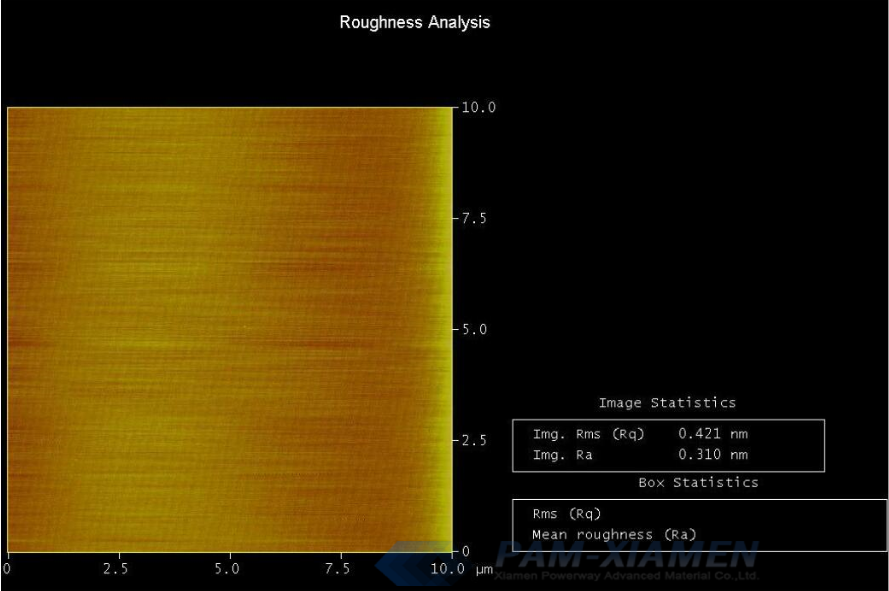
Q1: I have a question about your free standing GaN substrate. The RMS on Ga polar is around 2nm. What’s the AFM scan size of the RMS value? Or can you provide me with AFM images?
And the substrate is double side polished. Is it possible to make it only polished on the Ga polar side?
What’s your growth method for the free standing substrates (ex. HVPE)?
A:1/see attached AFM.
2/double side polished and single side polished are both available, you can only require single side polished.
3/Growth method: HVPE.
Q2:The main problem with the double side polished gallium nitride wafers is the reflection of the heating radiation and hence the MBE manipulator should be warmed at a higher temperature to obtained the desired temperature on the opposite face of the substrate (that where the growth itself takes place). a grounded face absorbs more efficiently heat.
A:One solution is to coat molybdenum in the backside of frestanding GaN to deal with optical reflection absorbtion.
Q3:In MBE is a custom procedure to degas the wafers in the buffer chamber before introducing them in the growth chamber. The degassing can be done at different temperatures, the higher the better and the shorter. However, increasing temperature could deteriorate the surface (GaAs wafers are degassed at 400 Celsisus in the buffer but could be heat at 600 under As atmosphere in the growth chamber; Silicon could be degassed at 850 in the buffer etc.). The point is: which is the maximum temperature one can degas the free-standing GaN substrate in the buffer chamber without affecting its surface (perhaps in the growth chamber the oxide removal temperature could be done at a higher temperature under nitrogen atmosphere)? Do you have such knowledge?
A:The best temperature for GaN degassed is between 750deg.-800deg. However, in 800 degree requires a very skilled operator to make sure the surface is not decomposition, therefore our propose temperature is 750 deg. Please see attached two pictures, which shows he surface RHEED pattern in different temperature (please review these two in order).
Q4:In the lack of an ICP process, how alse i could clean the FS GaN wafer before both the Ti deposition on the back side and for later growth by MBE?
A:A-IBE etching process is also suitable for the surface cleaning; however the etching thickness of GaN wafer should be less than 100nm.
Q5: Could you please tell me the name of the measuring instrument that measures TTV and Warp of GaN wafer?
A: We use a capacitive sensor back pressure measurement system to measure TTV and Warp of GaN wafer, the system has two probes, one is used to measure the front of the wafer, the other is used to measure the back of the wafer. When it comes close to touching the surface of the wafer, it measures it by air pressure. The accuracy can be controlled within 1 micron.
Q6: What is the XRD of freestanding GaN substrate?
A: The typical value of XRD(0002) of FS GaN substrate is 40arcsec; the typical value of XRD(10-12) is 48arcsec.
Q7: I would like to ask what is the corresponding Si doping concentration when the resistivity of Si doped freestanding GaN substrate is less than 0.04 ohm.cm?
A: Too much doping of Si for FS GaN substrate has an impact on its surface quality, while too little doping will result in high resistivity. To obtain specific doping concentration value, please contact victorchan@powerwaywafer.com.
Q8: I am ready to place an order for two 4″ n-doped Freestanding GaN wafers, but wanted to check if you guys could make one of them N-face CMP instead of the standard Ga-face CMP? Or both sides CMP would be acceptable…
A: Please kindly order GaN FS substrate with Ga face CMP. For N face CMP quality is not as good as Ga face.
Q9: This is my first time using free-standing GaN (as opposed to templates). We would first like to cut one wafer into pieces (1cm x 1cm). But eventually we would like to do some cleaving of those pieces to get good sidewalls for our laser research.
Do you have any guidance on the best process to cleave the wafer, and in which direction(s) it is possible?
A: If using laser cutting, there are burning marks on the edge of freestanding GaN substrate. It’s better to scribble with a blade.
For more information, please contact us email at victorchan@powerwaywafer.com and powerwaymaterial@gmail.com.