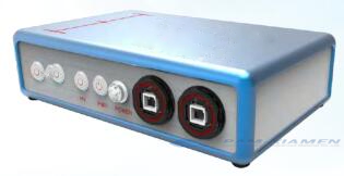
PAM-01A is a single channel preamplifier. It can be used as a key part for semiconductor detector, including CZT and Si, or others, including scintillator and gas.
1. Charge Sensitive Pre-amplifier Specification
Power Consumption
<0.43W
Power
±12V
Output Resistance
50 Ω
Equivalent Noise
ENC: 130e–
Working temperature
-20℃-+40℃
Falling edge time
250 ~ 400us
Input charge range
<1000fc
Gain
G=10mv/fc
Dimension
100×76×44mm3
Weight
265g
2. Charge [...]
2019-04-25meta-author
CONGRESSIONAL RESEARCH ARM PRODUCES REPORT ON THE U.S. CHIP INDUSTRY
A newly released report by a non-partisan research arm of Congress underscores how semiconductors’ economic and military importance has made the industry’s health a focus of congressional interest for nearly 70 years. The report, produced by the [...]
2016-07-20meta-author
High-power broad-area InGaNAs/GaAs quantum-well (QW) edge-emitting lasers on GaAs substrates in the 1200 nm range are reported. The epitaxial layers of the InGaNAs/GaAs QW laser wafers were grown on n+-GaAs substrates by using metal-organic chemical vapor deposition (MOCVD). The thickness of the InGaNAs/GaAs QW layers [...]
PAM XIAMEN offers8″ Silicon Wafer-3
Silicon Wafer
P-Type
Diameter 200.00±0.5 mm
Thickness 725±50μm
Dislocation density < 10-2 cm-2
Dopant – Boron
Resistivity- 10-40 Ω.cm
Notch SEMI STD
Chamfer width 250-350μm
Orientation – (100)±0.5
single sided polishing
For more information, please visit our website: https://www.powerwaywafer.com,
send us email at sales@powerwaywafer.com and powerwaymaterial@gmail.com
With more than 25+years experiences in compound semiconductor material field and [...]
2019-09-20meta-author
PAM-XIAMEN can offer InGaSb material substrate, which can be used for InGaSb photodetectors, InGaSb/GaAs quantum dots (QDs), InGaSb-on-insulator for p-MOSFET, and InGaSb/InAs superlattice materials for infrared photodiodes in the very long-wavelength infrared (VLWIR) range
It can be grown on GaAs substrate, GaSb (111)A substrate and [...]
2020-05-15meta-author
We investigated the effects of the substrate off-angle on the m-plane GaN Schottky diodes. GaN epitaxial layers were grown by metal–organic chemical vapor deposition on m-plane GaN substrates having an off-angle of 0.1, 1.1, 1.7, or 5.1° toward . The surface of the GaN epitaxial layers on [...]
2019-12-16meta-author