PAM-XIAMEN is able to supply epitaxial thin film of P-type GaN on GaN substrate. P-type GaN thin film epitaxial on GaN substrate is the main technique for developing emitting device. Mg is the most common p-type dopant in III-nitride material systems, partly due to the established activation process. High p-type doping of Mg concentration (1018/cm3) will be achieved in GaN when Mg dopant is diffused during the epitaxial growth. The Mg doping thin films grown show high resistivity, but it changes into the p-type conductivity by thermal activation. In 1990, Nakamura came up that the Mg-doped GaN into p-type conductivity is activated with thermal annealing, and the hole concentration obtained is 3×10¹⁸/cm3 and mobility is 9 cm2 /Vs. Doping by diffusion is one traditional IC processing technology. Rubin et al. got the p type GaN through diffusion of Mg. Through this method, the hole concentration obtained is 2×10¹⁶/cm3 and the mobility is 12 cm2 /Vs.
1. About Mg P-type Doping Concentration in GaN Epitaxial Wafer
The whole Mg-doped GaN epi wafer structure (PAM160608-GAN) we discuss below is:
Substrate: GaN c-face N-type grown by HVPE
Epi layer:
first layer undoped GaN 2um (Si, C, O <1E16cm-3);
second layer Mg-doped 1E17cm-3 4um GaN (Si, C, O <1E16cm-3).
Q: We would like to know how large the doping deviation is? And how high other contamination is such as Si, O, and C?
Mg-doping deviation in GaN on GaN epi wafer is +/- 10% or 20% or more.
Si, C, O doped level is <1E16cm-3 or less.
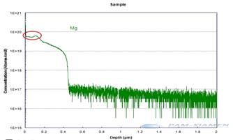
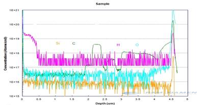
A: SIMS data shows as following figure that the impurity background levels for GaN on GaN epi wafer should be Si~1E16 or lower (SIMS detection limit), C~3~5E16, O~3~5E16 (could also be due to detection limit). These levels should be general for all systems.
Please note: Regarding the Mg doping concentration, technically it does have some trouble.
In general, we have a higher concentration of a Mg-doped (about 1019cm-2), to obtain a device hole concentration substantially acceptable (about 1017cm-2), such a design mainly from two considerations:
(a) Mg doping hole activation rate is very low, only 1%;
(b) In MOCVD material growth, backing doped (Si, O, C) in 1 ~ 3 * 1016cm-3, wherein Si, O will produce corresponding electron concentration (activation rate close to 100%, the corresponding electron concentration of about 1016cm-3), C elements are formed some deep level, it will reduce the concentration of electrons and holes;
But in any case, when the hole doped than backing a large magnitude, the GaN epitaxial material is still showing overall P-type conductivity characteristics.
2. Challenges for P-type GaN Thin Film Doping Technique
In the case that Mg p-type doping concentration is 1E17cm-3, and Si, C, O doping concentration is <1E16cm-3.
By doping, it will indeed be able to accurately control the doping concentration of Mg at 1017cm-3, the deviation can be controlled generally between 1 ~ 3 * 1017cm-3, but the presence of two such samples grown significant problem:
(a) Further Si, C, O doping concentration is reduced to 1016cm-3 or less, for MOCVD growth, it is a huge challenge.
(b) Even if the Si, C, O doping concentration is reduced to 1015cm-3, this time with the backing of the doped hole concentration Mg-doped (Si, O, C) concentration in the same order of magnitude, the growth of the obtained P-type GaN on GaN material is difficult to exhibit characteristics due to mutual compensation holes and electrons, and C elements from deep-level compensation effect brought about, the material has a great probability high impedance characteristics.
Unless the backing (Si, O, C) to reduce the doping concentration of 1014cm-3, to obtain a GaN epi on GaN substrate with hole concentration of 1015cm-3 is possible.
So, if you wants to Mg doping concentration at 1017cm-3, to obtain a hole concentration 1015cm-3, we believe that the larger obstacles in the art.
Of course, you can gradually reduce the doping concentration of Mg, for example, 1018cm-3, to obtain lower hole concentration, but there is a lack of detailed experimental data.
The program is still relatively safe use of higher Mg doping concentration (about 1019cm-2), to obtain an acceptable hole concentration (about 1017cm-2).

For more information, please contact us email at victorchan@powerwaywafer.com and powerwaymaterial@gmail.com.