PAM XIAMEN offers 2.5″ PBN Heater
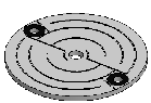
2.5″ PBN Heater.
1. Resistance: 22-35 ohm
2. Voltage: 180 V
3. Current: 15 A
4. Power: 2000 W

For more information, send us email at sales@powerwaywafer.com and powerwaymaterial@gmail.com
2.5″ PBN Heater.
1. Resistance: 22-35 ohm
2. Voltage: 180 V
3. Current: 15 A
4. Power: 2000 W
For more information, send us email at sales@powerwaywafer.com and powerwaymaterial@gmail.com
We are an expert of semiconductor wafers in semiconductor industry, and we offer technology support and wafers selling for thousands of univerisities and industrial customers by our decades experience, including Cornell University, Stanford Univeristy,Peking University, Shandong Univerity, university of south carolina,Caltech Faraon lab (USA),University of California, Irvine (USA),Singapore MIT Alliance for Research and Technology Centre (SMART),West Virginia University,Purdue Univerity, University of California, Los Angeles,King Abdullah University of Science & Technology,Massachusetts Institute of Technology,University of Houston,University of Wisconsin,University of Science and Technology of China etc. And now we show one article example as follows, who bought our wafers or service: Article title: Frequency Comb Generation From Stimulated Brillouin Scattering and Semiconductor Laser Diodes Published by: (Electrical Engineering) in The [...]
PAM XIAMEN offers FZ & MCZ silicon ingot and silicon wafer: Description Growth Method — MCZ Single crystal size inch 2 – 8 Conductivity Type — N P Doped elements — P/Sb B Crystal Orientation — <111> <110> <100> <111> <110> <100> Resistivity Ω.cm 0.0015-100 0.001-100 RRG % 20 20 Oxygen Concentration atoms/cm3 1.00E+18 1.00E+18 Carbon Concentration atoms/cm3 5.00E+16 5.00E+16 Diameter mm 55-157 55-157 Length mm 50-500 50-500 Dislocation EA/cm2 N/A N/A Swirl(After Oxidation) — N/A N/A Remarks:The above parameters can be customized. FAQ about MCZ Silicon Wafers Q:This is just a curiosity, but let me ask about the production method of [...]
PAM-XIAMEN can offer GaAs epiwafer (gallium arsenide epiwafer) with p-type & n-type AlGaAs multilayer for VCSEL laser application. The specifications of GaAs epiwafer are as follow: 1. Specifications of GaAs Epiwafer with AlGaAs Multilayers VCSEL, 980nm, GaAs epiwafer, 4″size PAM210208 Layer No. Material Group Repeat Mole Fraction(x) Strain(ppm) PL(nm) Thickness(nm) Dopant 32 GaAs – – – – – 156 C 31 Al(x)GaAs – – 0.04 – – 50.5 C 30 Al(x)GaAs – – 0.87->0.04 – – 20 C 29 Al(x)GaAs – – 0.87 – – 59.7 C 28 Al(x)GaAs – 16 0.04->0.87 – – 20 C 27 Al(x)GaAs – 0.04 – – 51.5 C 26 Al(x)GaAs – 0.87->0.04 – – 20 C 25 Al(x)GaAs – 0.87 – – 59.7 C 24 Al(x)GaAs – – 0.04->0.87 – – 20 C 23 Al(x)GaAs – – 0.04 – – 32.9 C 22 Al(x)GaAs – – 0.80->0.04 – – 20 C 21 Al(x)GaAs – – 0.98 – – 20 C 20 Al(x)GaAs – – 0.8 – – 61.6 C 19 GaAsP – – – – – – UD 18 In(x)GaAs – – – – 970nm – UD 17 GaAsP – – – – – – UD 16 In(x)GaAs – – – – 970nm – UD 15 GaAsP – – – – – – UD 14 In(x)GaAs – – – – 970nm – UD 13 GaAsP – – – – – – UD 12 Al(x)GaAs – – 0.87 – – 59.7 Si 11 Al(x)GaAs – – 0.04->0.87 – – 20 Si 10 Al(x)GaAs – – 0.04 – – 51.5 Si 9 Al(x)GaAs – – 0.87->0.04 – – 20 Si 8 Al(x)GaAs – 6 0.87 – – 59.7 Si 7 Al(x)GaAs – 0.04->0.87 – – 20 Si 6 Al(x)GaAs – 0.04 – – 51.5 Si 5 Al(x)GaAs – 30 0.92->0.04 – – 20 Si 4 Al(x)GaAs – 0.92 – – 59.8 Si 3 Al(x)GaAs – 0.04->0.92 – – 20 Si 2 Al(x)GaAs – 0.04 – – 51.5 Si 1 GaAs – – – – – 500 Si 4 inch GaAs substrate Si doped; [...]
PAM XIAMEN offers single crystal LiTaO3. LiTaO3 X-cut LiTaO3 optical grade, X-cut, 10x10x0.5mm, 2 SP LiTaO3 saw grade, X-cut, 10x10x0.5mm, 1sp LiTaO3 saw grade, X-cut, 3″ Dia x 0.5mm wafer, 1sp LiTaO3, 4″ wafer, specific parameters as follows: 4″ LT Wafer Specification Diameter 100.0±0.5mm Orientation Flat (OF) 30±2mm Second Refer. Flat [...]
Silicon wafers contribute significantly to the photovoltaic module cost. Kerfless silicon wafers that grow epitaxially on porous silicon (PSI) and are subsequently detached from the growth substrate are a promising lower cost drop-in replacement for standard Czochralski (Cz) wafers. However, a wide technological processing [...]
PAM XIAMEN offers KTaO3 Potassium Tantalate Crystal Substrates. Formula KTaO3 Point group m3m Cell parameters 0.3984nm Melting point 1352.2 ℃ Density 7.025 g/cm3 Mohs hardness 6 Growth method Czochralski method Refractive index 2.226@633nm, 2.152@1539nm Coefficient of thermal expansion 4.027 x 10⁻⁶/K Specific heat (temperature J/(K g) 0.378 Transparent bands (nm) 380~4000 Crystal orientation <100>, <110>, <111> Regular size 20x20x0.5mm, 10x10x0.5mm, 5x5x0.5mm, other sizes are available upon request For more information, please visit our website: [...]
| Cookie | Duration | Description |
|---|---|---|
| cookielawinfo-checkbox-analytics | 11 months | This cookie is set by GDPR Cookie Consent plugin. The cookie is used to store the user consent for the cookies in the category "Analytics". |
| cookielawinfo-checkbox-functional | 11 months | The cookie is set by GDPR cookie consent to record the user consent for the cookies in the category "Functional". |
| cookielawinfo-checkbox-necessary | 11 months | This cookie is set by GDPR Cookie Consent plugin. The cookies is used to store the user consent for the cookies in the category "Necessary". |
| cookielawinfo-checkbox-others | 11 months | This cookie is set by GDPR Cookie Consent plugin. The cookie is used to store the user consent for the cookies in the category "Other. |
| cookielawinfo-checkbox-performance | 11 months | This cookie is set by GDPR Cookie Consent plugin. The cookie is used to store the user consent for the cookies in the category "Performance". |
| viewed_cookie_policy | 11 months | The cookie is set by the GDPR Cookie Consent plugin and is used to store whether or not user has consented to the use of cookies. It does not store any personal data. |