PAM-XIAMEN can supply AlN on Sapphire wafers, more specifications you can find in: https://www.powerwaywafer.com/aln-single-crystal-substrate-template-4.html
At present, metal organic chemical vapor deposition (MOCVD) is considered one of the most widely used epitaxial techniques for AlN, but it always faces problems such as long growth cycles, high costs, and low substrate selection due to high growth temperatures. Compared with MOCVD, the preparation of AlN single crystal thin films by reactive magnetron sputtering, as an alternative technology, has advantages such as low equipment and process costs, no by-products during growth, and low impurity content. However, due to the inherent low mobility of Al atoms, the columnar growth mode of AlN during magnetron sputtering can lead to the generation of dislocations and defects.
1. Significance of Studying Structure and Optical Properties of Magnetron-Sputtered AlN
In recent years, Mie University in Japan has proposed a process combining magnetron sputtering with high-temperature annealing to improve the quality of AlN crystals. However, the impact of high-temperature annealing on the crystal plane orientation and optical properties of magnetron sputtered AlN is still unclear. In depth research on the structural and optical properties changes of magnetron sputtered AlN on sapphire substrates with different crystal planes after high-temperature annealing will help to further clarify and indicate the roadmap for the growth of ultra wide bandgap semiconductor materials based on magnetron sputtering technology, laying the foundation for improving the efficiency of deep ultraviolet optoelectronic devices.
2. Structure and Optical Properties of Magnetron-Sputtered AlN on Sapphire
Researchers deposited AlN thin films on sapphire substrates with different crystal plane orientations such as (0001), (10-10), and (11-20) using magnetron sputtering technology, and annealed them at 1700 ℃. The results showed that the crystallization quality of AlN thin films was greatly improved after high-temperature annealing. After high-temperature annealing, the half width at half maximum of the AlN (0002) rocking curve deposited on the c-plane and a-plane sapphire was as low as 68 and 151 arcseconds, respectively, which was several times lower than before annealing. In addition, after high-temperature annealing, due to the decrease in point defect density, the absorption band edge of AlN film shifts blue and the deep ultraviolet transmittance increases.
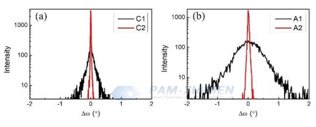
Fig. 1 High resolution XRD rocking curves of AlN (0002) orientation sputtered on sapphire substrates on c-plane (a) and a-plane (b) before and after high-temperature annealing (C1 and A1 are before annealing, and C2 and A2 are after annealing.)
| Table 1. AlN bandgap width calculated by the α2 versus photon energy curve | ||
| Sapphire substrate orientation | Before high-temperature annealing | After high-temperature annealing |
| a-plane | 6.109eV | 6.126eV |
| c-plane | 6.107eV | 6.114eV |
| r-plane | 6.069eV | 6.081eV |
The improvement of the structure and optical properties of magnetron sputtering AlN demonstrates the enormous potential of high-temperature annealing to achieve high-quality AlN on semi polar and non-polar substrates. This technology provides a possibility for the preparation of large-sized, high-quality non-polar and semi polar surface ultraviolet luminescent devices: in such a structure, the spontaneous polarization intensity is significantly reduced, thereby avoiding the problem of device efficiency degradation caused by uneven distribution of electrons and holes in space.

For more information, please contact us email at victorchan@powerwaywafer.com and powerwaymaterial@gmail.com.