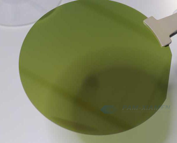
Silicon carbide (SiC) materials have significant advantages in key characteristics such as bandgap width and critical breakdown field strength, and can be used to make high voltage Schottky diodes. Currently, 650V-1700V SiC Schottky diodes are widely used in consumer, industrial, automotive and other fields. Schottky diode array based on SiC have higher energy efficiency, higher power density, smaller size, and higher reliability, which can break the limit of silicon in the field of power electronics technology and become the preferred device for new energy and power electronics. PAM-XIAMEN is able to provide SiC epitaxy for the preparation of Schottky diodes, with the specific structure as follows:
1. Schottky Diode Epitaxial Structure on SiC
Epitaxial layer: N-drift (lightly doped), mainly used to bear reverse voltage resistance
Substrate layer: N+(heavily doped), exhibiting resistance characteristics and lacking voltage tolerance
In order to enhance product competitiveness, the structure of silicon carbide Schottky diodes has also evolved from the standard Schottky barrier diode (SBD) structure (Fig. 1a) to junction barrier Schottky diode (JBS). The so-called JBS involves injecting a P-well on the surface of the epitaxial layer (Fig. 1b). When the device is subjected to back pressure, a depletion layer is formed around P through the P-well and N-, reducing leakage current and improving the reverse voltage resistance of the device.
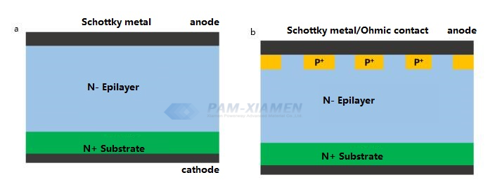
Fig. 1 Schematic Diagram of Schottky Diode Structure: a. SBD; b. JBS
2. How Does A Schottky Diode Work?
The basic structure of a Schottky diode is shown in Fig 1a. Essentially, when a metal and semiconductor material come into contact, the energy band at the interface semiconductor bends, forming a Schottky barrier. Metal and semiconductor coming into contact, electrons will run from the semiconductor into the metal. As a semiconductor loses electrons, it becomes positively charged, forming a space charge region (composed of immovable positive ions), which prevents the semiconductor’s electrons from continuing to move towards the metal, forming a Schottky barrier.
When a forward bias voltage is applied at both ends of the Schottky barrier (the anode metal is connected to the positive pole of the power supply, and the N-type substrate is connected to the negative pole of the power supply), the Schottky barrier layer narrows, its internal resistance decreases, and forward conduction occurs. On the contrary, if a reverse bias is applied at both ends of the Schottky barrier, the Schottky barrier layer becomes wider, its internal resistance increases, and the reverse cutoff occurs.
3. SiC Schottky Diode Application
SiC Schottky diodes can be widely used in high-power fields such as switching power supplies, power factor correction (PFC) circuits, uninterruptible power supplies (UPS), photovoltaic inverters, etc. They can significantly reduce circuit losses and improve the working frequency of circuits.
In the PFC circuit, replacing the original silicon fast recovery diode (FRD) with SiC SBD can make the circuit operate above 300kHz, while the efficiency remains basically unchanged. In contrast, the efficiency of circuits using silicon FRD decreases sharply above 100kHz. As the working frequency increases, the volume of passive components such as inductors decreases correspondingly, and the volume of the entire circuit board decreases by more than 30%.

For more information, please contact us email at victorchan@powerwaywafer.com and powerwaymaterial@gmail.com.