SiC wafers are available for power electronics, scientific or industrial applications, specifications as: https://www.powerwaywafer.com/sic-wafer/sic-wafer-substrate.html
SiC is a binary compound formed in a 1:1 ratio of Si and C elements, consisting of 50% silicon (Si) and 50% carbon (C). Its basic structural unit is the Si-C tetrahedron.
1. SiC Crystal Structure Arrangement
1.1 Si-C Tetrahedron Structure
The Si-Si bond energy is 310 kJ/mol, which can be understood as the force required to pull apart these two atoms. The higher the bond energy, the greater the force required to pull apart. The atomic spacing of Si-C bond is 1.89 Å, and the bond energy is 447 kJ/mol. From the bond energy, it can be seen that compared to traditional silicon-based semiconductor materials, silicon carbide based semiconductor materials have more stable chemical properties. From the graph, it can be seen that any C atom is connected to the nearest four Si atoms, while conversely, any Si atom is bonded to the nearest four C atoms.
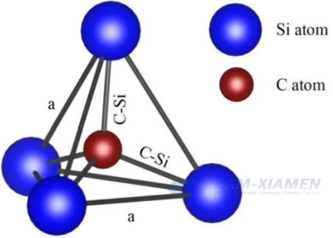
Fig. 1 Schematic diagram of Si-C tetrahedral structure of SiC crystal
1.2 SiC Layered Structure
The SiC crystal structure can also be described using the layered structure method, as shown in the Fig. 2. Several C atoms in the crystal occupy hexagonal lattice sites on the same plane, forming a C atom dense layer, while Si atoms also occupy hexagonal lattice sites on the same plane, forming a Si atom dense layer. Each C in the C atomic packing layer is connected to the nearest Si, and vice versa, the Si atomic packing layer is also the same. Every two adjacent layers of C and Si atoms form a carbon silicon double atomic layer. The arrangement and combination of SiC crystals are very diverse, and more than 200 SiC crystal forms have been discovered so far.
In order to distinguish the different crystal forms of SiC, the Ramsdell method is currently mainly used for labeling. This method uses a combination of letters and numbers to represent the different crystal forms of SiC. The letters are placed at the end to indicate the type of crystal cell. C represents cubic crystal form, H represents hexagonal crystal form, and R represents rhombic crystal form. The number is placed at the beginning to indicate the number of layers of Si-C diatomic layers in the basic repeating unit. Except for 2H-SiC and 3C-SiC, all other crystal forms can be regarded as a mixture of sphalerite and wurtzite structures, namely a densely packed hexagonal structure.
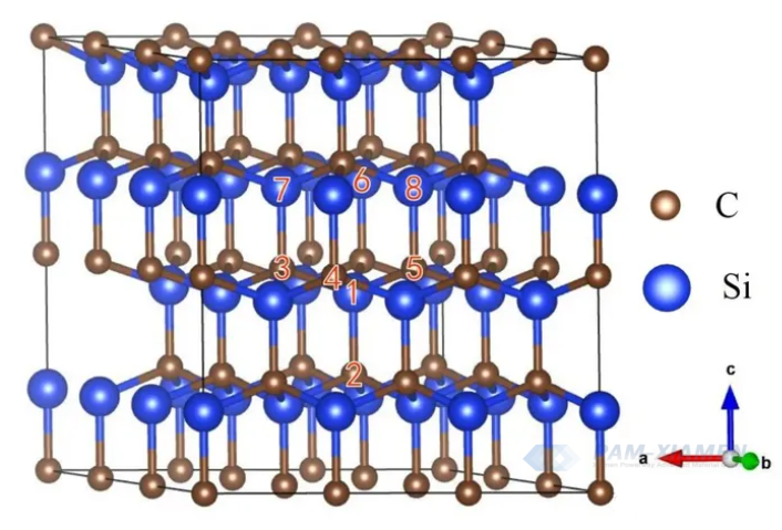
Fig. 2 SiC crystal layered structure
2. What Are C-Plane and Si-Plane of Silicon Carbide Wafer?
The C-plane refers to the (000-1) crystal plane of a SiC wafer, which is the surface cut by the crystal along the negative direction of the c-axis. The terminal atom on this surface is carbon atoms. The silicon surface refers to the (0001) crystal plane of a silicon carbide wafer, which is the surface cut along the positive direction of the c-axis of the crystal. The terminal atom on this surface is silicon atoms.
The difference between the C-plane and the silicon plane can affect the physical and electrical properties of SiC wafers, such as thermal conductivity, conductivity, carrier mobility, interface density of states, etc. The selection of C-plane and Si-plane can also affect the manufacturing process and performance of SiC devices, such as epitaxial growth, ion implantation, oxidation, metal deposition, contact resistance, etc.
3. Application of C-Plane and Si-Plane of SiC Wafer
During the growth process of SiC crystal, due to differences in atomic arrangement density and chemical stability between the Si and C surfaces, they exhibit different characteristics in material processing and device preparation.
The Si face usually has better electron mobility and is suitable as a channel layer for power electronic devices.
While the C face may exhibit better performance, such as higher thermal conductivity, in certain specific scientific or industrial applications.

For more information, please contact us email at victorchan@powerwaywafer.com and powerwaymaterial@gmail.com.