Slicing, cleaning and kerf analysis of germanium wafers machined by wire electrical discharge machining
This paper investigates the slicing of germanium wafers from single crystal, gallium-doped ingots using wire electrical discharge machining. Wafers with a thickness of 350 μm and a diameter of 66 mm were cut using 75 and 100 μm molybdenum wire. Wafer characteristics resulting from the process such as the surface profile and texture are analyzed using a surface profiler and scanning electron microscopy. Detailed experimental investigation of the kerf measurement was performed to demonstrate minimization of material wastage during the slicing process using WEDM in combination with thin wire diameters. A series of timed etches using two different chemical etchants were performed on the machined surfaces to measure the thickness of the recast layer. Cleaning of germanium wafers along with its quality after slicing is demonstrated by using Raman spectroscopy.
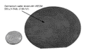
Fig. 1. Germanium wafer with a thickness of 350 μm sliced with WEDM.
Source: Journal of Materials Processing Technology
If you need more information about Slicing, cleaning and kerf analysis of germanium wafers machined by wire electrical discharge machining, please visit our website:https://www.powerwaywafer.com/, send us email at sales@powerwaywafer.com or powerwaymaterial@gmail.com