PAM XIAMEN offers 8″ FZ Prime Silicon Wafer.
1. Specification of 8″ FZ Prime Silicon Wafer
8″ 200+/-0.2 mm
Double Side Polished
Prime FZ N type
resistivity 8000-14000Ωcm
orientation 100 ±0.5°
Thickness 625 +/- 5µm
Laser Mark None or SEMI
edge profile SEMI
Notch SEMI
Oi content 11-15 PPMA
warp 35
Bow 35
Site Flatness SFQD 20X20mm: 0.40um
TTV 6 µm
backside treatment Polished
LPDs >= 0,30 µm (including COP’s) <=25
LPDs >= 0,20 µm (including COP’s) <=30
LPDs >= 0,16 µm (including COP’s) <=60
Surface Metals (Al,Ca,Cu,Fe,Ni,Zn,Cr,Na) Max 5E10/cm2
Metrology edge exclusion(lpd’s, mechanical parameters) 3 mm
2. FAQ of FZ Silicon Wafer
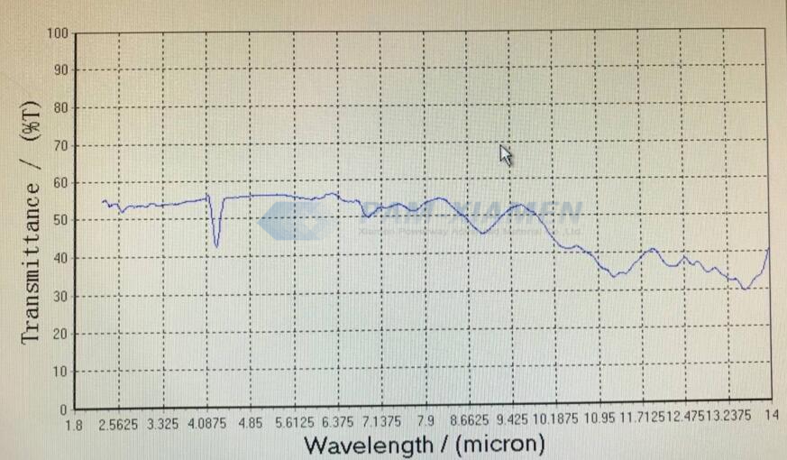
Q1: Do you have the transmission spectrum (or n, k values) of the FZ Si wafers at infrared wavelengths, e.g. 2 to 14 um?
A: The transimission spectrum of the FZ Si wafers at infrared wavelengths of 2 to 14 um is shown as below:
Q2: What is the thickness of the 8″ FZ wafer you measured transmission spectrum (if it is different from what you quoted)?
A: Applied to the thickness of FZ silicon which <10mm
For more information, please contact us email at victorchan@powerwaywafer.com and powerwaymaterial@gmail.com.
Found in 1990, Xiamen Powerway Advanced Material Co., Ltd (PAM-XIAMEN) is a leading manufacturer of semiconductor material in China. PAM-XIAMEN develops advanced crystal growth and epitaxy technologies, manufacturing processes, engineered substrates and semiconductor devices. PAM-XIAMEN’s technologies enable higher performance and lower cost manufacturing of semiconductor wafer.
You can get our free technology service from enquiry to after service based on our 25+ experiences in semiconductor line.