Abstract
Advanced characterisation plays an important role for further improvements of the cost effectiveness ($/Wp) of solar cells. This paper presents an overview of advanced characterisation techniques that are presently being used for the analysis of silicon wafer solar cells, either in the laboratory or in the factories. Techniques covered include
luminescence imaging, lifetime spectroscopy, and optical and electrical measurements. We present a detailed loss analysis, entirely based on measured parameters, that quantifies the main loss processes in silicon wafer solar cells.This loss analysis is completely based on high-precision measurements and provides a detailed quantification (in
W/cm2) of the power losses of the solar cell due to front metal shading, front surface reflection of the active area,front surface escape, series and shunt resistance, non-perfect active-area internal quantum efficiency, and the forward-bias current at the one-sun maximum power point. We also show that a thorough characterisation of the
individual processing steps and a detailed loss analysis of the final solar cells can be used to improve the average efficiency and yield of industrial silicon wafer solar cells.
1. Introduction
Silicon wafer solar cells currently dominate the market and their market share is even increasing. The overwhelming majority of these solar cells are produced by a fabrication sequence consisting of the following steps:
i. Surface texture including saw damage removal
ii. Phosphorus diffusion (either tube or inline diffusion)
iii. Phosphorus silicate glass removal
iv. Silicon nitride deposition
v. Screen printing of front and rear metal contacts
vi. Edge isolation
For every industrial solar cell, its solar energy conversion efficiency will be measured. However, a significant amount of information can be obtained from the silicon samples prior to and after completion of the silicon wafer solar cell. In this paper some typical process related issues are presented that can beextracted from partly processed silicon wafers. In addition, a bottom-up loss analysis for a finished silicon wafer solar cell is presented that quantifies the seven most important loss mechanisms. This method
can serve as a guide in the optimisation of silicon wafer solar cells.
2. Characterisation of partly processed silicon wafers
2.1. Raw wafer analysis by photoluminescence imaging
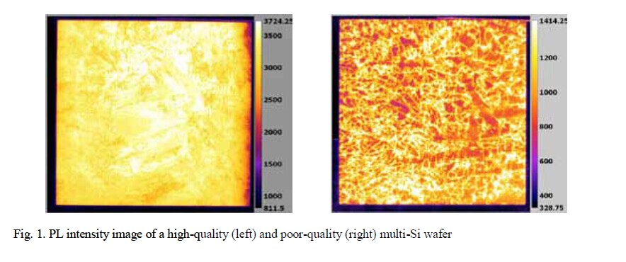
Photoluminescence (PL) imaging has emerged in the last decade as a very versatile characterisation technique in the field of silicon wafer photovoltaics [1]. Of particular interest is that PL enables us to study partly processed silicon wafers in every step of the solar cell fabrication sequence. As an example, Fig. 1 shows PL intensity images taken on a high-quality and a low-quality multi-Si wafer (PL images taken with the LIS-R1 system from BT Imaging, Australia). The wafers were measured in their as-received state, i.e. no processing step was applied at SERIS. The high-quality wafer has a uniform appearance, apart from a lower intensity edge at the right which can be attributed to the block-casting process. The low-quality wafer has a clearly different appearance with a significant portion of the wafer appearing “dark”. It has been shown by Giesecke et al. that dark areas in raw wafers relate to areas with bulk minority carrier lifetimes of < 10 s [2]. Interestingly, the areas close to the grain boundaries are brighter in the PL image of the low-quality multi-Si wafer. This can be explained by the internal gettering of impurities by the grain boundaries, resulting in higher effective lifetimes in the proximity of grain boundaries in multi-Si with a high impurity content. This multi-Si wafer was clearly cut from either the top or bottom of the ingot. This result clearly shows that PL has the potential to assess the quality of as-received wafers before any processing. This information can be used for incoming quality control or to “bin” the incoming wafers into quality groups and to tailor especially the thermal processing in order to get the optimal cell efficiency for each quality group, instead of processing all wafers in the same way.
2.2. Saw damage removal and texturing
The as-received silicon wafers contain a defective layer at each surface (front and rear), as a result of the sawing process. The minority carrier lifetime in this saw-damaged layer is relatively low due to chemical impurities and crystal imperfections resulting from the sawing process. This defective layer is removed by chemical processing, typically in the same step that is used for texturing the surfaces of the silicon wafer. It is of key importance that the defective layer is completely removed in this chemical step.
However, the thickness of the defective layer varies between wafer suppliers, so a characterisation sequence is required to ensure that the defective layer is completely removed. In Fig. 2(a) a process flow is shown that allows the extraction of the minimal required saw damage etching (SDE) time for a particular silicon wafer type. Symmetrically passivated lifetime structures are prepared from Si wafers which have received various SDE times (KOH at 80oC). Subsequently the effective lifetime is determined by, for example, quasi-steady-state photoconductance decay (WCT-120, Sinton Consulting, USA) [3]). From Fig. 2(b) we can see that the minimal SDE time is 4 minutes for this particular type of wafer.
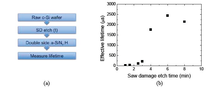
Fig. 2. (a) Experimental process flow used to determine the minimal saw damage etching time required for a silicon wafer; (b) The effective minority carrier lifetime of the symmetrically passivated lifetime sample increases significantly for increasing saw damage etching time. For this type of Si wafer, a minimal saw damage etching time of 4
minutes should be used.
2.3. Phosphorus diffusion
The standard way for the emitter formation is phosphorus diffusion, either by inline or tube diffusion.The main parameters of interest from the P diffusion are the absolute value of the sheet resistance and its lateral uniformity. In Fig. 3 a sheet resistance map is shown that was obtained by taking 49 individual measurements with a four point probe (Crestbox, Napson, Japan) on a mono-Si wafer. For this specific wafer the uniformity is relatively poor, which can lead to contacting issues in the front Ag metallisation.The mono-Si wafers were loaded back-to-back in this case, to minimise dopant diffusion into the rear surface of the wafer. However, the PL intensity image shows a high-intensity edge around the wafer that can be attributed to parasitic P diffusion at the rear of the wafer. Hence, this parasitic diffusion should be taken into account in the remainder of the solar cell fabrication sequence, as it could result in shunting of the cell or a poor contact or passivation at the rear.
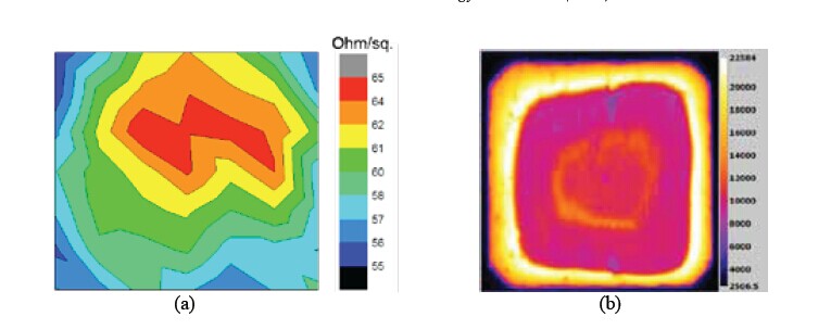
Fig. 3. (a) Measured sheet resistance distribution of a 156 mm wide pseudo-square n+ diffused p-type mono-Si wafer with a target sheet resistance of 60 Ohm/square. A clear non-uniformity is observed, which can cause problems in later stages of the solar cell fabrication; (b) The PL intensity image of the same wafer furthermore reveals significant
non-uniformities at the rear of the wafer related to the non-optimal back-to-back loading of the wafers into the tube diffusion process.
2.4. Silicon nitride deposition
Silicon nitride is currently the state-of-the-art antireflection coating (ARC) for silicon wafer solar cells, as the film reduces reflection losses and simultaneously provides bulk and surface passivation. It is well known that the best level of surface passivation does not always coincide with the best ARC properties of the film; hence, both properties should be addressed in parallel. In Fig. 4 the ARC and surface passivation properties are plotted as a function of the refractive index of the silicon nitride (SiNx) film. The optical absorption and reflection losses were determined by a combination of ray tracing and the transfer matrix method, as described in detail in Ref. [4]. It can be seen that it is important to consider both reflection and absorption losses induced by the silicon nitride film on textured mono-Si wafers. The transmission of the film should be optimised as this is this limits the obtainable current of the solar cell.

Fig. 4. (a) Weighted average reflection, absorption and transmission as a function of the refractive index of the SiNx film on alkaline textured mono-Si wafers. The optical thickness of the SiNx film was kept constant at 150 and the reflection, absorption and transmission were modelled using ray tracing in combination with the transfer matrix method. The optical losses were weighted by the photon flux of the AM1.5G spectrum; (b) Emitter saturation current density measured by photoconductance decay on SiNx-passivated textured mono-Si wafers with a 70 Ohm/sq n+ diffusion on both sides, as a function of the refractive index of the SiNx film.
With respect to surface passivation, it can be seen that a range of silicon nitride films provide a good level of surface passivation on an n-type emitter, but that care should be taken if the film is stable under a standard industrial firing. By combining both the ARC and passivation properties the best silicon nitride film can be selected (in this case a silicon nitride film with a refractive index of 2.0).
2.5. Screen printing and firing
The front and rear metal contact of a typical Si wafer solar cell are formed by screen printing and subsequent co-firing of the contacts in a firing furnace. The challenge is to obtain a low series resistance in combination with a low spatially averaged charge carrier recombination at the front and rear of the solar cell. Moreover, the metallisation fraction at the front of the solar cell should be minimised. Severe contacting issues can easily be picked up by monitoring the fill factor and series resistance of the cell (see
Section 3), however, some process issues require spatially resolved characterisation to be detected. In Fig. 5 two electroluminescence (EL) intensity images are shown for Si wafer solar cells with contacting issues at the front and rear of the solar cell. The width of the front metal grid lines is constantly being reduced to reduce the metallisation fraction at the front of the solar cell. However, this can lead to an increase in series resistance caused by the line conductance or disconnected fingers. From Fig. 5(a) it can
be seen that broken fingers can very easily be picked up by EL imaging. Contacting and/or passivation issues of the back contact can also easily be picked up from EL images, see Fig. 5(b). In this specific case a mirror image of the metal belt of the firing furnace is visible in the image, hence, the non-optimal firing results in localised poor contacting at the back thereby reducing the fill factor of the solar cell.
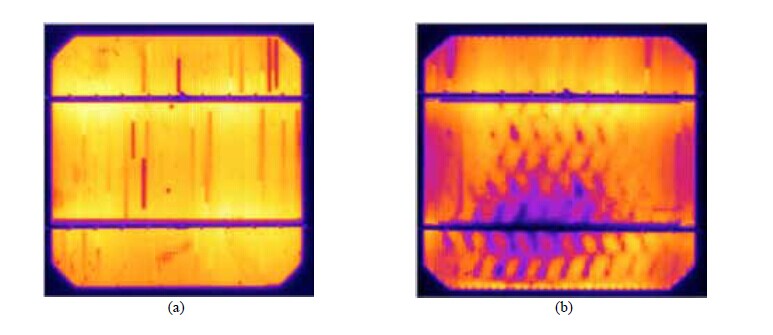
Fig. 5. (a) EL intensity image of a mono-Si wafer solar cell with broken Ag front fingers; (b) EL intensity image of a mono-Si wafer solar cell with a poor rear Al contact.
3. Characterisation of finished solar cells
For all solar cells the one-sun I-V curve is measured and the energy conversion efficiency determined.However, for solar cell researchers it is of key importance to know which factors are limiting the efficiency of a given solar cell. For this reason a novel method was developed at SERIS that performs a bottom-up loss analysis for Si wafer solar cells and quantifies the seven most important loss mechanisms of a solar cell at the 1-sun maximum power point (MPP), assuming that the series resistance corrected MPP voltage (Vmpp) of the cell remains constant [5]. This analysis is thus not intended to quantify the losses relative to the theoretical (but practically not attainable) solar cell efficiency limit. Instead, it is intended to be used in an iterative way, by determining the dominant loss mechanisms in a particular solar cell, then fabricating an improved version of the solar cell, then repeating the loss analysis, and so on. The loss analysis method is demonstrated here on an 18.1% efficient p-type Cz mono-Si wafer solar cell
fabricated at SERIS. The cell has a homogeneous n-type emitter at the front surface and a full-area Alalloyed back surface field layer at the rear surface. Both the Ag front and Al rear contact were screen printed. The loss mechanisms investigated in the SERIS loss analysis are:
Front metal grid shading
Front surface reflectance in the active area;
Front surface escape
Series resistance
Shunt resistance
Non-perfect quantum efficiency
Diode recombination
First, the electrical properties of the solar cell are determined. In this work a one-sun I-V tester (SolSim-210, Aescusoft, Germany) with a super-class-A solar simulator (WXS-220S-L2, Wacom, Japan) was used. From the light J-V curve (not shown here) the standard solar cell parameters are derived: Opencircuit voltage Voc, short-circuit current density Jsc, fill factor FF, efficiency Eff, maximum power point voltage Vmpp and maximum power point current density Jmpp. From the dark J-V curve the shunt resistance
is determined by a linear fit in the -50 mV to 50 mV range. By shifting the one-sun J-V curve by Jsc from the fourth to the first quadrant (shown in Fig. 6) and assuming that the solar cell obeys the superposition principle, the series resistance at the one-sun maximum power point (Rs.light) is determined from the voltage difference between the dark and the shifted one-sun J-V curve at Impp, as described by Aberle et al. [6]. Furthermore, the effective diode saturation current density J0.eff and the effective ideality factor neff are determined from the Rs-corrected light J-V curve. All these derived values are summarised in Table 1.
.jpg)

The quantum efficiency of the solar cell is determined in this work with the differential spectral response method, using a combination of modulated monochromatic light with steady-state white bias light [7]. The system used in this work (Fimo-210, Aescusoft, Germany) has a filter wheel based monochromator with 34 narrow-band filters and the linearity of the cell is checked prior to the measurement. The external and internal quantum efficiency for the metal-free area of the solar cell are shown in Fig. 7.
The metallised area of the cell’s front surface was measured using an automated 3D vision measurement system (MeasurVision, Sunny Instruments, Singapore). The reflectance Raa of the active cell area is subsequently calculated from the measured hemispherical reflectance (Lambda 950, PerkinElmer, USA), the measured metallisation fraction of the front surface, and the measured reflectance of the used front metal grid. The IQE of the active area (IQEaa) is then calculated using the measured metallisation fraction of the cell and the calculated Raa of the metal-free area. The IQEaa is used below for the quantification of the recombination losses in the short-circuited cell.
In the final part of the analysis the power losses (in mW/cm2) at the MPP of the solar cell are calculated for each of the seven studied loss mechanisms, assuming that the cell obeys the superposition principle. The optical losses and the losses due to a non-perfect IQEaa are calculated by weighting the measured data with the AM1.5G spectrum, whereby the calculated current loss at short circuit is converted into a power loss at MPP by multiplication with Vmpp. The resistive losses and the forward bias
current are calculated at MPP conditions, using the measured values of the solar cell from Table 1 and the one-diode equivalent circuit model. Our analysis thus assumes that the difference between Jsc and Jmpp is entirely due to the additional recombination triggered in the device by the forward bias voltage, which is true if the cell obeys the superposition principle and the shunt resistance is sufficiently high. The power loss results of this analysis are given in Table 2. As mentioned above, the analysis assumes that the series resistance corrected maximum power point voltage remains constant. It can be seen that for this particular cell the power loss due to the non-perfect IQEaa is dominant (37%), followed by the power loss due to front metal shading (24%). It can also be seen that the total current loss at MPP (12.6 mA/cm2) combined
with the measured Jmpp adds up to 47.2 mA/cm2, which is very close to the total possible current from the AM1.5G spectrum for wavelengths up to 1200 nm (47.0 mA/cm2). Hence, all major photon current loss processes have been accounted for.
4. Conclusions
In this paper we have shown that a significant amount of information can be extracted from partly processed silicon wafers, by applying a range of characterisation techniques. Furthermore we have presented a power loss analysis method for silicon wafer solar cells which quantifies the seven main power loss mechanisms at the cell’s maximum power point based on a bottom-up analysis. The method assumes that the Vmpp of the cell remains constant when the various loss mechanisms are eliminated; thus,
it should be used iteratively when improving solar cells, as the Vmpp will change as well. This analysis can easily be adapted to other photovoltaic technologies such as Si thin film, CIGS, and CdTe based solar cells, and to photovoltaic modules. As described in this paper, advanced characterisation plays a key role in improving the efficiency and yield of photovoltaic technologies.
References
[1] Trupke T, Bardos RA, Schubert MC, Warta W. Photoluminescence imaging of silicon wafers. Appl. Phys. Lett. 2006; 89:044107.
[2] Giesecke JA, The M, Kasemann M, Warta W. Spatially resolved characterization of silicon as-cut wafers with photoluminescence imaging. Prog. Photovolt. 2009; 17: 217.
[3] Sinton RA, Cuevas A. Contactless determination of current-voltage characteristics and minority-carrier lifetimes in semiconductors from quasi-steady-state photoconductance data. Appl. Phys. Lett. 1996; 69:2510.
[4] Duttagupta S, Ma F, Hoex B, Mueller T, Aberle AG. Optimised antireflection coatings using silicon nitride on textured silicon surfaces based on measurements and multidimensional modelling. Proc. International Conf. on Materials for
Advanced Technologies 2011, Symposium O, Singapore; Energy Procedia, 2011.
[5] Aberle AG, Zhang W, Hoex B. Advanced loss analysis method for silicon wafer solar cells. Proc. SiliconPV 2011 Conf. (1st International Conf. on Crystalline Silicon Photovoltaics), Freiburg, Germany; Energy Procedia, 2011, volume 8, p. 244-9.
[6] Aberle AG, Wenham SR, Green MA. A new method for accurate measurements of the lumped series resistance of solar cells. Proc. 23rd IEEE Photovoltaic Specialists Conf., Louisville, USA; 1993, p. 133-8.
[7] Metzdorf J. Calibration of solar cells. 1: The differential spectral responsivity method. Appl. Optics 1987; 26: 1701
Source:Sciencedirect
For more information, please visit our website:www.powerwaywafer.com, send us email at sales@powerwaywafer.com or powerwaymaterial@gmail.com