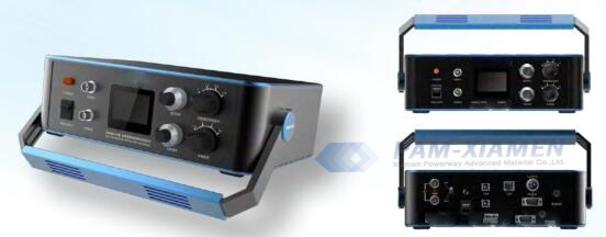
Indium antimonide (InSb) detector is sensitive for the mid-wave infrared (MWIR) band. In terms of mid-infrared detection in the 3-5um band, due to the advantages of mature material technology, high sensitivity and good stability, InSb detectors stand out from detectors based on other materials. [...]
2022-04-06meta-author
PAM XIAMEN offers CeO2 Epi-thin film on YSZ Alloy.
CeO2 Film (40 nm one side) on YSZ <100> 10x10x0.5 mm
CeO2 Film (40 nm one side) on YSZ <110> 10x10x0.5 mm.
CeO2 Film (40 nm one side) on YSZ, <111>10x10x0.5 mm, 1sp
Due to [...]
2019-04-26meta-author
MOS SiO2/GaN structures were fabricated with different surface preparation and different PECVD processes for the dielectric thin film deposition (ECR-PECVD and ICP-PECVD in continuous and pulsed modes). On the basis of C-V curves, the surface preparation steps, involving chemical etching with BOE, UV-Ozone oxidation [...]
PAM-XIAMEN can supply silicon wafers to meet your application demands, more wafer specifications please visit: https://www.powerwaywafer.com/silicon-wafer.
The purity, surface flatness, cleanliness and impurity contamination of semiconductor silicon wafers have an extremely important influence on the chips. The local flatness of silicon wafer is one of [...]
2022-09-20meta-author
PAM XIAMEN offers test grade silicon wafers
Below is just a short list of the test grade silicon substrates!
Inches
Cust class
Dopant
Type
Orientation
PFL length
PFL direction
SFL
Off orientation
Resistivity
Diameter
Thickness
Bow
TTV
Warp
6
SSP
Arsenic
N+
100
57,5 ± 2,5
110 ± 1
0.0 ± 1.0 °
0.0028-0.0035 Ohmcm
150 ± 0.5 mm
440 ± 20 µm
40
5
40
6
SSP
Arsenic
N+
111
57,5 ± 2,5
110 ± 1
4.0 ± 0.5 °
< 0.0035 Ohmcm
150 [...]
2019-02-25meta-author
PAM XIAMEN offers 4″FZ Prime Silicon Wafer-9
4″ Silicon Wafer
Orientation (100)
Thickness 525±25μm
SSP
P type, Boron doped
Resistivity>200Ωcm
Roughness<8 Angstrom
For more information, send us email at sales@powerwaywafer.com and powerwaymaterial@gmail.com
2020-06-11meta-author