We are an expert of semiconductor wafers in semiconductor industry, and we offer technology support and wafers selling for thousands of univerisities and industrial customers by our decades experience, including Cornell University, Stanford Univeristy,Peking University, Shandong Univerity, university of south carolina,Caltech Faraon lab (USA),University of California, Irvine (USA),Singapore MIT Alliance for Research and Technology Centre (SMART),West Virginia University,Purdue Univerity, University of California, Los Angeles,King Abdullah University of Science & Technology,Massachusetts Institute of Technology,University of Houston,University of Wisconsin,University of Science and Technology of China etc.
And now we show one article example as follows, who bought our wafers or service:
Article title:
Tailoring the structural and optical characteristics of InGaN/GaN multilayer thin films by 12 MeV Si ions [...]
2019-12-02meta-author
PAM XIAMEN offers6″ FZ Silicon Wafer-5
Silicon wafers, per SEMI Prime, P/E 6″Ø×875±25µm,
FZ p-type Si:B[111]±0.5°, Ro > 10,000 Ohmcm,
Warp<60μm,
One-side-polished, Particles: ≤10@≥0.3μm,
MCL (Na, Al, K, Fe, Ni, Cu, Zn)<5E10/cm²,back-side etched,
Tarnish, orange peel, contamination, haze,
micro scratch, chips, edge chips, crack,
crow feet, pin hole, pits, dent, waviness,
smudge&scar on [...]
2019-09-19meta-author
PAM XIAMEN offers 4″ Silicon Wafer.
Material
Orient.
Diam.
Thck
(μm)
Surf.
Resistivity
Ωcm
Comment
p-type Si:B
[100]
4″
2100
P/E
1-100
SEMI Prime, Manual Edges
p-type Si:B
[100]
4″
3000
P/P
1-10
SEMI Prime
p-type Si:B
[100]
4″
3175
P/P
1-10
SEMI Prime, TTV<8μm
p-type Si:B
[100]
4″
3200
P/E
1-100
SEMI Prime, Sealed as group of 9 wafers
p-type Si:B
[100]
4″
4000
P/P
1-100
SEMI Prime
p-type Si:B
[100]
4″
4000
P/P
1-100
SEMI Prime
p-type Si:B
[100]
4″
5000
P/E
1-100
Prime, NO Flats
p-type Si:B
[100]
4″
890 ±15
P/P
0.5-10.0
SEMI TEST (Scratches), TTV<8μm
p-type Si:B
[100] ±0.2°
4″
300
P/P
0.1-0.3
SEMI Prime
p-type Si:B
[100] ±1°
4″
490 ±5
P/P
0.1-1.0
SEMI Prime, TTV<0.8μm
p-type Si:B
[100]
4″
525
P/E
0.1-0.2
SEMI Prime
p-type Si:B
[100]
4″
350
P/E
0.095-0.130
SEMI Prime
p-type [...]
2019-03-05meta-author
The FZ (float zone) gas-phase doped silicon single crystal with high purity, few defects, low compensation, and low oxygen and carbon content can be supplied by PAM-XIAMEN. It is widely used in various high-sensitivity detectors and low-loss microwave devices. To get more specifications of [...]
2022-08-16meta-author
We investigated the effect of the thickness of a 3C-SiC buffer layer on the growth of GaN on a Si substrate. GaN samples with thicknesses of 2.0 and 4.5 µm were grown by metal organic vapor phase epitaxy. Islands were observed at the initial [...]
2018-08-14meta-author
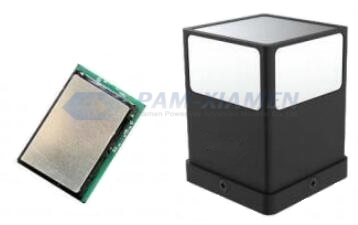
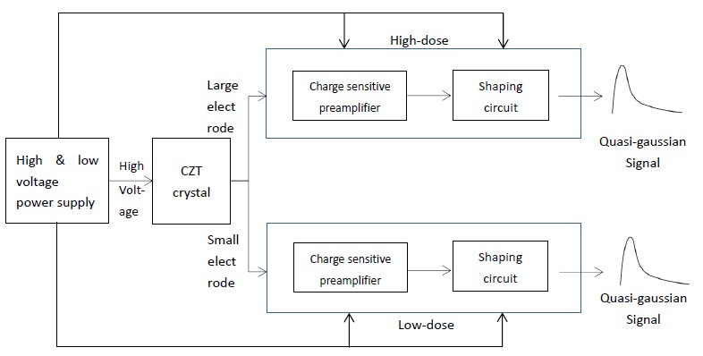
PAM XIAMEN offers CZT and MCT crystal.
CZT and MCT crystal are new semiconductors which enables effective conversion of radiation to electron. The technology will reform radiography and radiation measurement in medical and industrial areas. We both provides the standard substrate , CZT and [...]
2019-04-19meta-author