Semiconductor GaAs materials are mainly used in optical communication active devices, semiconductor light emitting diodes (LEDs), high-efficiency solar cells, and Hall devices. Moreover, GaAs optoelectronic devices have important applications in household appliances, industrial instruments, large screen displays, office automation equipment, traffic management, etc. To grow GaAs single crystals, GaAs polycrystals are needed. PAM-XIAMEN can supply polycrystalline gallium arsenide. See the following table for specific parameters of GaAs polycrystalline wafer:
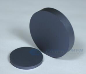
1. Specification of GaAs Polycrystalline Wafer
| Main Parameters for GaAs Polycrystal Wafer | |
| Growth Method | Horizontal Method |
| Purity | 7N (99.99999%) |
| Size | 2” & 4” |
| Thickness | 400um~25mm |
| Resistivity | >1E7 Ohm.cm |
| Mobility | >6700 cm2/V.s |
| Surface Finished | As-cut or DSP |
GaAs polycrystalline wafer can be used for growing GaAs single crystal.
In addition, the polycrystalline wafer can be used as infrared window material. And studies found that polycrystalline GaAs infrared window coating with anti-reflection (AR) will have better transmittance.
2. Challenges and Solutions for Polycrystalline GaAs Synthetized by Horizontal Method
Because gallium arsenide is a binary compound, the vapor pressure of arsenic is high, and gallium and arsenic are easy to oxidize, the synthetic polycrystal of GaAs is prone to defects such as quartz deformation, polycrystal oxidation and gallium-rich tail. In order to overcome these defects, we can optimize the raw material formula, arsenic vapor pressure control and furnace cooling temperature field design. Specific as follows:
1) In terms of raw material, in addition to strictly ensuring that the molar ratio of gallium to arsenic is 1:1, an additional 0.5% molar ratio of arsenic is added.
2) Arsenic vapor pressure control is mainly used to observe the status of arsenic vapor in the quartz tube and the shape of the quartz tube wall through the furnace body window, so as to adjust the arsenic sublimation rate. If the arsenic vapor in the quartz tube appears dense fog and the quartz tube shows signs of expansion, it indicates that the arsenic vapor pressure is too high, at this time, the temperature at the arsenic end can be appropriately reduced by 5~8℃ to slow down the arsenic sublimation rate. On the contrary, if the arsenic vapor in the quartz tube is thin and the quartz tube shrinks, the temperature at the arsenic end can be appropriately increased by 5~8 ℃, accelerating the sublimation of arsenic and restore the original complete shape of quartz tube.
3) For the problem of quartz tube cracking and polycrystalline oxidation caused by furnace cooling, the optimization design of temperature cooling program at high temperature end is mainly adopted. After the synthesis of gallium and arsenic, the heating wire at the high temperature end can not be cooled at the same time, but starts from the first heating wire near the middle temperature zone. The slow cooling process gradually releases the internal stress of the quartz tube, thus avoiding the occurrence of cracking and even bursting during the cooling process of the quartz tube.
The poly gallium arsenide obtained after the optimized process has obvious metallic luster, no oxidation on the surface, and no rich gallium exists at the cut end. The parameters of mobility and carrier concentration obtained is conform to the requirements of GaAs single crystal preparation.
Remark:
The Chinese government has announced new limits on the exportation of Gallium materials (such as GaAs, GaN, Ga2O3, GaP, InGaAs, and GaSb) and Germanium materials used to make semiconductor chips. Starting from August 1, 2023, exporting these materials is only allowed if we obtains a license from the Chinese Ministry of Commerce. Hope for your understanding and cooperation!

For more information, please contact us email at victorchan@powerwaywafer.com and powerwaymaterial@gmail.com.