GaN template with single side polished and atomic step is available, which is grown on 4H or 6H SiC C-axis (0001) substrate. GaN growth on SiC substrate can achieve lower thermal expansion, lower lattice mismatch, and excellent thermal conductivity, thereby giving full play to the characteristics of GaN. Due to better heat dissipation, GaN on SiC substrate is very suitable for manufacturing low-energy, high-power devices. Following is the detailed specification of GaN-on-SiC epitaxial wafer:
1. Specification of GaN on SiC Substrate
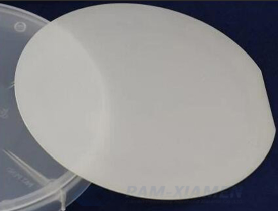
Item 1:
P-GaN wafers on SiC template (PAMP20230-GOS)
GaN on SiC, p type
2″ dia, p -type,
Thickness : 2um
Orientation: C-axis(0001)+/-1.0°
XRD(102)<300arc.sec
XRD(002)<400arc.sec
Substrate: SiC substrate, semi-insulating, C(0001)
Structure: GaN on SiC(0001).
Single Side Polished, Epi-ready, with atomic steps
Item 2:
GaN on SiC, (2”) 50.8±1mm (PAM200818-G-SIC)
u-GaN wafers on silicon carbide template
GaN layer thickness: 1.8um
GaN layer: n type, Si doped
XRD(102)<300arc.sec
XRD(002)<400arc.sec
Single side polished,Epi-ready, Ra<0.5nm
Carrier concentration: 5E17~5E18.
2. About GaN on SiC Epitaxy
High quality 6H-SiC wafer is an ideal substrate for growing GaN epitaxy. The residual strain effect on the interface can be reduced because of the nearly perfect lattice match. GaN epi-layer grown on SiC can be grown by MBE, MOCVD and sandwich sublimation techniques. Among them, using the sandwich sublimation to grow GaN thin film on 6H SiC substrate has better quality of crystalline and optical properties than that grown by MBE and MOCVD.
Researches by GaN on SiC foundry show that the epitaxial surface morphology and photoluminescence of GaN on SiC substrate is strongly affected by the substrate polarity. The polarity of (0001) GaN is changing with the polarity of SiC substrate basal plane. When the substrate uses C as the end plane, a C-N bond is formed between the C atom and the N atom. There is a small overlap between the bottom of the conduction band and the top of the valence band at the Fermi level, and a pseudo-energy gap appears, which is reflecting the strong bond-forming effect among each atom. And its interface binding energy is -5.5489eV, which is slightly larger than the binding energy of the interface structure of Si atom TOP bit adsorbing N -5.5786eV.
As the size of SiC substrates continues to expand, GaN epitaxial wafers with fewer defects and better quality will be grown.
3. Applications of GaN Epitaxial Growth on SiC Wafer Substrate
GaN and SiC have been extensively studied for high-efficiency power switching systems. Now, the GaN on SiC transistor has shown great performance and potential of the wide band gap material for power devices.
In addition, the high-power amplifier fabricated on GaN on SiC wafer can operate in the frequency range of 9 GHz to 10 GHz and is suitable for pulsed radar applications. The amplifier has a three-stage gain, can provide a large signal gain greater than 30 dB and an efficiency greater than 50%, can meet lower system DC power requirements, and provide support for simplifying system thermal management solutions. The GaN on SiC technology simplifies system integration and provides excellent performance. In short GaN on SiC substrate will play a major role in 5G applications.

For more information, please contact us email at victorchan@powerwaywafer.com and powerwaymaterial@gmail.com.