The Silicon crystal orientations that we often hear are <100>, <110> and <111>(shown as Fig. 1), respectively indicating a crystallographic family. The single crystal silicon structure belongs to cubic crystals, and the <100> crystal orientation family represents six crystal orientations: [100], [010], [001], [100], [0-10], and [00-1]. Therefore, we rarely hear crystal orientations such as <001>, <011>, and <101>, while <100>, <110>, and <111> crystal orientations are the most common. So why is it rare to hear crystal orientation families such as <200> and <311> with indices greater than 1? The reason is actually related to the atomic density and bond energy of the crystal plane. The distance between the crystal planes d is larger compared to other exponential crystal planes greater than 1. The atomic density of the crystal plane is higher, the distance between atoms is smaller, the bond energy is larger, and the stability of the crystal plane is higher. Therefore, the silicon crystal orientation <100>, <110>, <111> are commonly used for silicon substrates or epitaxy. PAM-XIAMEN manufactures silicon wafers with orientations of <100>, <110>, <111>, more specifications please refer to https://www.powerwaywafer.com/silicon-wafer.
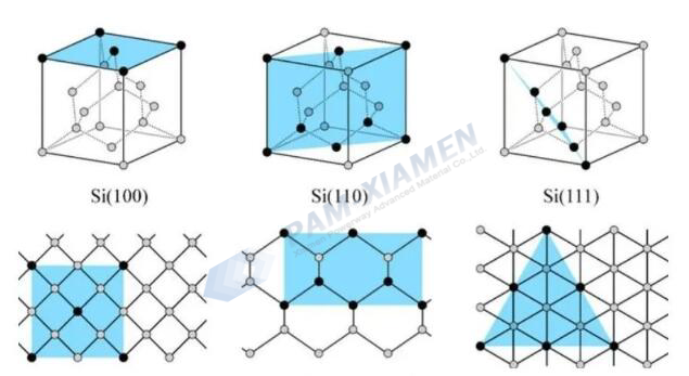
Fig. 1 Silicon Crystal Orientation: <100>, <110>, <111>
1. What Are the Characteristics of Silicon Crystal Orientation with <100>, <110> and <111>?
For the silicon crystal orientation <100>, atomic surface density=(1+4×1/4)/(a ^ 2)=2/(a ^ 2), crystal surface spacing d=a/√(h ^ 2+k ^ 2+l ^ 2)=0.543nm, atomic bond density n100=4/(a ^ 2);
For the <110> wafer crystal orientation, atomic surface density=(2+4×1/4+2×1/2)/(√2×(a ^ 2))=3.5/(a ^ 2), crystal surface spacing d=a/√(h ^ 2+k ^ 2+l ^ 2)=0.384nm, atomic bond density n110=3√2/(2×a ^ 2)=2.1/(a ^ 2);
For the silicon wafer with crystal orientation <111>, atomic surface density=(3×1/6+3×1/2)/(√3/2×(a ^ 2))=2.31/(a ^ 2), crystal plane spacing d=a/√(h ^ 2+k ^ 2+l ^ 2)=0.314nm, atomic bond density n111=2√3/(a ^ 2)=3.5/(a ^ 2);
The atomic density on the crystal plane decreases in the order of 111>110>100, so the diffusion rate and corrosion rate increase in the direction of 111<110<100. The corrosion rate on the 111 plane is about 1.48um/min, on the 110 plane it is about 3.0um/min, and on the 100 plane it is about 3.4um/min.
The oxidation rate is 111>110>100, which is due to the high surface density of 111 atoms, more unsaturated bonds, and faster binding with oxygen.
The atomic bond density on the <110> surface is the lowest, so silicon wafers with a <100> orientation are more prone to fragmentation, while wafers with a <100> orientation are more prone to fragmentation into 4 equal parts along the direction with the lowest atomic bond density, and wafers with a <111> orientation are more prone to fragmentation into 6 equal parts.
The cleavage plane of silicon is <111>, because <111> has the highest atomic surface density, naturally growing silicon crystals often have the outermost <111> crystal orientation.
2. Applications of <100>, <110> and <111> Crystal Oriented Silicon Wafers
2.1 <100> & <110> Crystal Oriented Silicon Wafers for MOSFET
<100> crystal oriented silicon substrates are often used for manufacturing power devices, such as MOSFETs. The reasons are illustrated as:
Power devices are generally surface channel devices, and the density of surface defect states has a significant impact on threshold voltage and reliability. The surface atomic surface density of (100) crystal plane is the smallest, corresponding to the lowest atomic surface density of states. There are fewer surface unsaturated bonds, and fewer defects are generated when the device surface oxidizes;
Due to the low density of the (100) crystal plane, its thermal oxidation and etching rates are relatively fast, and process experts have conducted more research on the <100> crystal orientation process.
Wafers with <100> or <110> are widely used crystal planes in MEMS. In the process of achieving corrosion, wet etching mainly relies on the difference in corrosion rates between different crystal planes. Adopting 100 plane wafer processing, using a mask along the <110> crystal direction, and etching in alkaline solution, it can achieve a {111} smooth surface with an angle of 54.7 degrees with the 100 plane wafer. It is commonly used in the production of structures such as pressure sensors. When wet etching 110 sided silicon wafers, it exhibits different characteristics from 100 sided silicon wafers. Etching on 110 plane silicon wafers produces {111} faces perpendicular to the substrate, which can provide a large area and high-quality optical surface, and has a wide range of applications in the optical field.
2.2 <111> Silicon Crystal Orientation for Bipolar Devices
<111> silicon crystal orientation is more commonly used in bipolar devices owing to:
Crystal structure: In the <111> crystal orientation, the crystal structure of silicon wafers has a special symmetry. This symmetry allows for better control of electron and hole movement in the manufacture of bipolar devices, resulting in better current control and performance, and allows for the production of very shallow doping;
Surface characteristics: The <111> crystal oriented atomic surface density is the highest, and the dissolution rate is the slowest. When making PN junctions, it is relatively easy to control and obtain a flat and stable junction surface, which is very important for manufacturing bipolar devices. A flat surface helps to manufacture precise electrodes and structures, reduce current leakage and electron tunneling effects, and improve device performance and reliability. In addition, the oxidation rate towards the <111> crystal orientation of silicon wafer is higher, which can reduce the oxidation time;
Coplanar device integration: Due to the good surface characteristics and symmetry of <111> oriented silicon wafers, the integration of coplanar devices can be easily achieved. Coplanar devices refer to devices where electrons and holes operate on the same chip. This design can reduce resistance and capacitance between devices, improve device speed and power efficiency.

For more information, please contact us email at victorchan@powerwaywafer.com and powerwaymaterial@gmail.com.