SiC wafer can be used to manufacture BJT (bipolar junction transistor) devices with low conduction resistance and high blocking voltage up to tens of kilovolts. For applications with a blocking voltage of 4.5kV and higher, bipolar SiC power devices will have more practical application value than unipolar SiC power devices. Compared with most field-effect transistors, BJT has higher carrier processing ability, lower conduction resistance, and is an important component of other bipolar devices. PAM-XIAMEN can grow SiC BJT epitaxial wafer to meet your applications. Take the following structure for example:
1. Basic Structure of BJT on 4H-SiC
| Epi layer | Thickness | Doping Concentration |
| n- contact | 40nm | 9×1019cm-3 |
| n- emitter | 100nm | 3×1019cm-3 |
| p- base | 140nm | 8×1018cm-3 |
| n- collector | 1000nm | 8×1015cm-3 |
| n- buffer layer | 700nm | 1×1019cm-3 |
| Semi-insulating 4H-SiC substrate | ~1018cm-3 |
2. What Is BJT?
BJT is an electronic device with three terminals made of three different doped semiconductors. The charge flow in the transistor is mainly due to the diffusion and drift motion of carriers at the PN junction. The operation of this type of transistor involves the flow of both electron and hole carriers, hence it is called bipolar and also known as bipolar carrier transistor.
According to polarity, it can be divided into PNP and NPN types:
NPN type SiC BJT transistor: consists of two layers of N-type doped regions and a layer of P-type doped semiconductor (base) between the two. The small current input to the base will be amplified, resulting in a larger collector emitter current. When the base voltage of an NPN type transistor is higher than the emitter voltage and the collector voltage is higher than the base voltage, the transistor is in a forward amplification state. In this state, there is a current between the collector and emitter of the transistor. The amplified current is the result of electrons injected into the base region by the emitter (which are minority carriers in the base region) drifting to the collector under the push of an electric field. Due to the higher electron mobility than hole mobility, most bipolar transistors currently used are NPN type.
PNP type SiC BJT: consists of two layers of P-type doped regions and a layer of N-type doped semiconductor between the two. The small current flowing through the base can be amplified at the emission end. That is to say, when the base voltage of a PNP transistor is lower than the emitter, the collector voltage is lower than the base, and the transistor is in the forward amplification region.
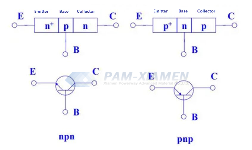
Fig.1 Schematic diagram of SiC BJT circuit symbol (arrows representing the direction of current inflow and outflow)
In many cases, SiC BJTs are easier to prepare than SiC power MOSFETs, and silicon carbide BJTs won’t encounter issues where the quality of the oxide layer seriously affects device characteristics. However, BJT is a current control device with higher input driving current and lower input impedance in the open state. This will result in additional power dissipation, complicating the design of the drive circuit.
3. Applications of SiC BJT
SiC BJT is generally applied in the following two aspects:
High voltage and high current applications: Due to their high withstand voltage and current carrying capacity, SiC BJT basic electronics have advantages in high voltage and high current applications, such as power transmission and distribution systems.
Linear applications: SiC BJT performs well in linear applications such as audio amplifiers and power management. They can provide lower distortion and higher linearity.

For more information, please contact us email at victorchan@powerwaywafer.com and powerwaymaterial@gmail.com.