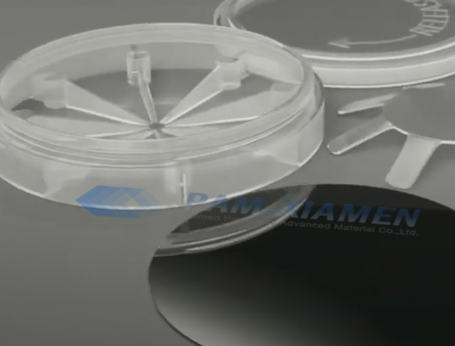
PAM-XIAMEN can offer 2&3 inches P-type GaAs substrates. Gallium arsenide (GaAs) is a III-V type direct band gap semiconductor with a zinc blend crystal structure, and GaAs p-type dopant is commonly used as a substrate for epitaxial growth of other III-V semiconductors, including indium gallium arsenide, aluminum gallium arsenide, etc.The parameters are shown in the table below:
1. Specification of 2 inch p-type GaAs substrates
PAM-190308-GAAS
| Parameter | Customer’s Requirements | Guaranteed/Actual Values | UOM | ||
| Growth Method: | VGF | VGF | |||
| Conduct Type: | S-C-P | S-C-P | |||
| Dopant: | GaAs-Zn | GaAs-Zn | |||
| Diameter: | 50.8±0.4 | 50.8±0.4 | mm | ||
| Orientation: | (100)0°±0.5° | (100)0°±0.5° | |||
| OF location/length: | EJ[0-1-1]±0.5°/16±1 | EJ|0-1-1]±0.5°/16±1 | |||
| lF location/length: | EJ[0-11]±0.5°/7±1 | EJ[0-11]±0.5°/7±1 | |||
| lngot CC: | Min:1E19 | Max:5E19 | Min:1.5E19 | Max:2.0E19 | /cm |
| Resistivity: | NA | NA | Ohm.cm | ||
| Mobility: | NIA | NA | cm2/vs | ||
| EPD: | Max:5000 | Min:900 | Max: 1100 | /cm2 | |
| Thickness: | 350±25 | 350±25 | μm | ||
| TTV: | Max:10 | Max:10 | μm | ||
| TIR: | Max:10 | Max: 10 | μm | ||
| Max: | Max:10 | Max:10 | μm | ||
| Warp: | Max: 10 | Max: 10 | μm | ||
| Surface-Finish-front: | Polished | Polisbed | |||
| Surface-Finish-back: | Etched | Etched | |||
| Epi-Ready: | Yes | Yes | |||
2. Specification of 3 inch p-type GaAs substrates
PAM-190315-GAAS
| Sr. No. | Parameter | Specification |
| 1. | Type of semiconductor | p-type (Zn or C doped), VGF grown |
| 2. | Diameter | 76.2+/-0.5 mm |
| 3. | Orientation | (100)±0.1°(may or may not be 2 degree off ) |
| 4. | Thickness | 500± 25um |
| 5. | Carrier density | 0.5 to 5x 10E19/cc |
| 6. | Corresponding Sheet resistance | Ohm/square |
| 7. | EPD | ≤5000 cm2 |
| 8. | Primary Flat | us(0-1-1)±0.2 degree/EJ |
| 9. | Major Flat Length | 22±2mm |
| 10. | Minor Flat Length | 11±2mm |
| 11. | Flat Orientation tolerance | ±0.02 degree |
| 12. | Surface finish | Polished one side |
| 13. | Laser Mark | Back surface along major flat |
| 14. | Packing | Individually Packed in inert atmosphere |
| 15. | Test report | Yes |
After Si, GaAs is a new type of semiconductor material with the deepest research and the most widely used. It has the characteristics of high mobility, large forbidden band width and high temperature resistance. The p-type conductivity GaAs substrates are mainly used in the fields of high-frequency communications, wireless networks and optoelectronics. With the development of process technology p-type gaas ohmic contact, the gallium arsenide substrates produced are getting larger in size, with a high geometric accuracy and a high surface quality.
For more information, please contact us email at victorchan@powerwaywafer.com and powerwaymaterial@gmail.com.