GaAs is a typical III-V direct bandgap semiconductor material with excellent optoelectronic properties and high mobility, making it suitable for the production of high-speed RF devices. GaAs can also form quantum well structures with GaAlAs, further improving the performance of light-emitting devices (low threshold current, narrow linewidth). The GaAs/GaAIAs thin film epitaxy material is currently the most widely used and early researched III-V semiconductor material, with mature processes and performance, suitable for making various types of photonic devices, including active and passive devices, and can therefore achieve single-chip integration of various photonic devices.
PAM-XIAMEN can provide GaAs-based wafers with custom-thickness AlGaAs layers to fabricate AlGaAs-based photonic integrated chips(PICs). Take the following thin-film epitaxial structure for example:
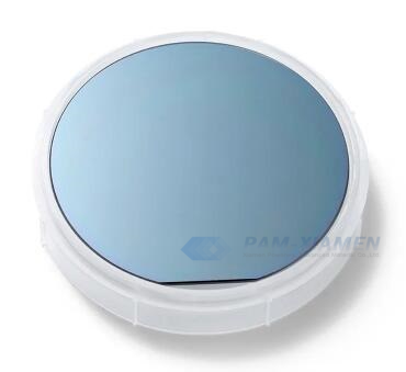
1. AlGaAs / GaAs Thin Film Epitaxy
| 4” GaAs Epitaxy Wafer with AlGaAs Layer (PAM210223-ALGAAS) | ||
| Layer No. | Epi Material | Thickness |
| 4 | GaAs | – |
| 3 | Al0.7Ga0.3As | – |
| 2 | Al0.2Ga0.8As | – |
| 1 | Al0.7Ga0.3As | 600nm |
| Substrate | GaAs | |
2. About Photonic Integrated Chips based on AlGaAs Epitaxial Films
PIC, also known as a photonic chip, is a microchip that includes two or more photonic components to form a functional circuit.
Researchers have attached AlGaAs epitaxy deposition thin film to silicon oxide substrates through hetero-integration, and used the latest breakthrough platform processing technology to provide waveguides with high refractive index contrast while greatly reducing waveguide propagation loss. As a result, the rate of quantum light sources has been increased by 1,000 times through resonant cavities formed by AlGaAs thin films epitaxial growth, and the efficiency is 1,000 times higher than any previous technology, enabling billions of entangled photon pairs to be created every second from a micro-watt laser beam, greatly improving the computing speed of quantum computers.
In addition to greatly improving the rate of photon sources, the power consumption required to achieve photon sources based on thin film epitaxy of AlGaAs has also been reduced from 1.4W to 100uW, and the volume has been reduced to smaller than a hair. The advantages of AlGaAs thin film epitaxial heterostructures in integrating laser diodes and other optical devices make it possible to design ultra-small size and highly integrated devices, effectively reducing the size and weight of components to meet practical applications.
Photonic integrated chips fabricated on thin film epitaxy can be used to create faster and more energy efficient devices. This is because thin film crystal epitaxial PICs can sense with the highest accuracy and are very effective in processing and transmitting data. They can also be integrated with traditional electronic chips and applications, covering a range of industries, including data and telecommunications, medical and healthcare, engineering, and transportation.
Remark:
The Chinese government has announced new limits on the exportation of Gallium materials (such as GaAs, GaN, Ga2O3, GaP, InGaAs, and GaSb) and Germanium materials used to make semiconductor chips. Starting from August 1, 2023, exporting these materials is only allowed if we obtains a license from the Chinese Ministry of Commerce. Hope for your understanding and cooperation!

For more information, please contact us email at victorchan@powerwaywafer.com and powerwaymaterial@gmail.com.