Silicon carbide (SiC) wafer are available, for more wafer information please click https://www.powerwaywafer.com/sic-wafer. The performance of SiC wafer slicing determines the processing level of subsequent thinning and polishing. Slicing is prone to cracks on the surface and subsurface of the SiC wafer, increasing the [...]
2022-08-05meta-author
Credit: MSU
A university-built small satellite known as the Cosmic X-Ray Background NanoSat-2 (CXBN-2) is being prepared for an ambitious upcoming science mission. The spacecraft – scheduled for launch into space on March 19 – is expected to deliver crucial data that could advance our [...]
2017-08-09meta-author
A template-based vision system for the 100% inspection of wafer die surfaces has been developed. Design goals included a requirement for the detection of flaws as small as two thousandths of an inch on parts up to 8-in. wafer size. Each die is treated [...]
PAM XIAMEN offers Te-Dy-Fe (Directionally solidified GMM).
Giant magnetostrictive material is an alloy made of terbium, dysprosium and iron by directional solidification. It can change electrical energy into mechanical action or vice versa because of its merit as being sensing and actuating material. Demanding [...]
2019-05-20meta-author
We are an expert of semiconductor wafers in semiconductor industry, and we offer technology support and wafers selling for thousands of univerisities and industrial customers by our decades experience, including Cornell University, Stanford Univeristy,Peking University, Shandong Univerity, university of south carolina,Caltech Faraon lab (USA),University of California, Irvine (USA),Singapore MIT Alliance for Research and Technology Centre (SMART),West Virginia University,Purdue Univerity, University of California, Los Angeles,King Abdullah University of Science & Technology,Massachusetts Institute of Technology,University of Houston,University of Wisconsin,University of Science and Technology of China etc.
And now we show one article example as follows, who bought our wafers or service:
Article title:Evidence for Deep Acceptor Centers in Plant Photosystem I Crystals
Published by:
Irina Volotsenko ; Michel Molotskii ; Anna Borovikova ; Nathan [...]
2019-12-09meta-author
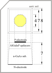
PAM XIAMEN offers 3″ Silicon Wafer.
Diameter
Type
Dopant
Growth
method
Orientation
Resistivity
Thickness
Surface
Grade
76.2
N
Phos
CZ
-100
1-20
950-1050
P/E
PRIME
76.2
N
Phos
CZ
-100
1000-1050
P/E
PRIME
76.2
N
Phos
CZ
-100
1-20
1975-2025
P/E
PRIME
76.2
N
Phos
CZ
-100
1-20
2900-3100
P/E
PRIME
76.2
N
Phos
CZ
-100
1-50
2900-3100
P/E
PRIME
76.2
N
Phos
CZ
-100
1-20
5900-6100
P/E
PRIME
76.2
N
Phos
CZ
-100
10-60
9900-10100
P/E
PRIME
76.2
N
Phos
CZ
-111
300-350
P/P
PRIME
76.2
N
Phos
CZ
-111
350-400
P/E
PRIME
76.2
N
Phos
CZ
-111
1975-2025
P/P
PRIME
76.2
N
Phos
CZ
-111
1-20
2900-3100
P/E
PRIME
76.2
N
Phos
CZ
-111
1-20
4900-5100
P/E
PRIME
76.2
N
Phos
CZ
-111
1-20
5900-6100
P/E
PRIME
76.2
N
Phos
CZ
-111
1-20
11900-12100
P/E
PRIME
76.2
N
Phos
CZ
-110
300-350
P/P
PRIME
76.2
N
Phos
CZ
-110
350-400
P/E
PRIME
76.2
P
Boron
CZ
-100
1-20
43768
P/P
PRIME
76.2
P
Boron
CZ
-100
1-20
40-60
P/P
PRIME
76.2
P
Boron
CZ
-100
1-20
80-100
P/P
PRIME
76.2
P
Boron
CZ
-100
1-20
140-160
P/P
PRIME
76.2
P
Boron
FZ
-100
>3000
300-350
P/P
PRIME
For more information, please visit our website: https://www.powerwaywafer.com,
send us email at sales@powerwaywafer.com and powerwaymaterial@gmail.com
Found in 1990, Xiamen Powerway Advanced Material Co., Ltd (PAM-XIAMEN) is a leading manufacturer of semiconductor material in China.PAM-XIAMEN develops advanced crystal growth and epitaxy technologies, [...]
2019-03-04meta-author