PAM XIAMEN offers 4″CZ Prime Silicon wafer-16
4″ CZ Silicon Wafer SSP
Silicon wafers, per SEMI Prime,
P/E 4″Ø×525±25μm, SEMI Flats (two),
p-type Si:B[100]±0.5°, Ro=(0.001-0.002)Ohmcm,
One-side-polished, back-side Alkaline etched,
TTV<5μm, Bow/Warp<30μm,
Wafers free of striation marks,
Sealed in Empak or equivalent cassette.
For more information, send us email at sales@powerwaywafer.com and powerwaymaterial@gmail.com
2021-01-06meta-author
PAM XIAMEN offers 4″ Silicon Wafer.
Diameter
Type
Dopant
Growth
method
Orientation
Resistivity
Thickness
Surface
Grade
100
N
Phos
CZ
-100
1-20
500-550
P/E/WTOx
100
N
Phos
CZ
-100
1-50
2900-3100
P/E
PRIME
100
N
Phos
CZ
-100
50-70
4850-5050
P/E
PRIME
100
N
Phos
CZ
-100
1-50
5900-6100
P/E
PRIME
100
N
Phos
CZ
-100
>10
9900-10100
P/P
PRIME
100
N
Phos
CZ
-111
1-10
4000-6000
P/E
PRIME
100
N
Phos
FZ
-111
> 20000
275-325
P/E
PRIME
100
N
Phos
FZ
-111
> 20000
275-325
P/P
PRIME
100
N
Phos
FZ
-111
2000-4000
275-325
P/P
PRIME
100
N
Phos
CZ
-111
450-500
P/P
PRIME
100
N
Phos
FZ
-111
> 20000
475-525
P/P
PRIME
100
N
As
CZ
-111
.001-.005
500-550
P/E
PRIME
100
N
Phos
CZ
-111
1-20
500-550
P/E
PRIME
100
N
Phos
FZ
-111
2000-4000
500-550
P/P
PRIME
100
N
Phos
CZ
-111
1-20
4800-5200
P/E
PRIME
100
N
Phos
CZ
-111
1-3
11300-11500
P/E
PRIME
100
N
Phos
CZ
-110
450-500
P/P
PRIME
100
N
Phos
CZ
-110
1-20
500-550
P/E
PRIME
100
P
Boron
CZ
(100)-4
0.01-0.02
175-225
P/P
PRIME
100
P
Boron
CZ
(100)-4
0.01-0.02
200-250
P/E
PRIME
100
P
Boron
CZ
(100)-4
0.01-0.02
325-375
P/P
PRIME
For more information, please visit our website: https://www.powerwaywafer.com,
send us email at sales@powerwaywafer.com and powerwaymaterial@gmail.com
Found in 1990, Xiamen Powerway Advanced Material Co., Ltd (PAM-XIAMEN) is a leading manufacturer of semiconductor material in China.PAM-XIAMEN develops advanced crystal growth [...]
2019-03-04meta-author
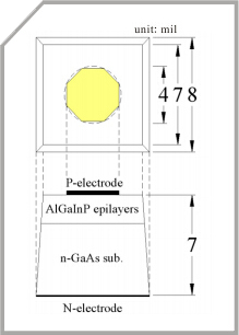
PAM XIAMEN offers 905nm laser diode wafers.
1. Specs of 905nm Laser Diode Wafer
1.1 Three Stark 905nm Pulse LD Structures PAM211202-GAINAS
Layer
Composition
Thickness
Concentration
13
P+ GaAs
/
/
12
P-AlGaAs cladding + waveguide
d~1.6um
/
11
Undoped GaInAs QW PL:880~900nm
/
/
10
N- AlGaAs cladding + waveguide
/
9
N++ GaAs/P++ GaAs Tunnel junction
/
/
8
P- AlGaAs cladding + waveguide
/
7
Undoped GaInAs QW PL:880~900nm
/
/
6
N- AlGaAs cladding [...]
2019-03-13meta-author
PAM-XIAMEN can offer 6 inch N-type GaAs wafer. Gallium arsenide is a second-generation semiconductor material with excellent performance. Gallium arsenide belongs to the second-generation semiconductors, which has far superior frequency, power and withstand voltage performance than the first-generation silicon semiconductors. According to different resistance, GaAs [...]
2021-04-20meta-author
PAM XIAMEN offers 4″CZ Prime Silicon Wafer Thickness 525 ± 25 µm.
PRIME WAFERS SILICIUM CZ
DIAMETER 4 inch (100mm+/-0.5mm)
ORIENTATION <1-0-0> +/-1°
THICKNESS : 525µm +/-25µm
SSP
TTV < 10µm – BOW < 40µm
FLAT : 32.5mm
TYPE P
RESISTIVITY : 8 – [...]
2019-07-05meta-author
PAM-XIAMEN offers (11-22) Plane Si-GaN Freestanding GaN Substrate
Item
PAM-FS-GAN(11-22)- SI
Dimension
5 x 10 mm2 or 5 x 20 mm2
Thickness
380+/-50um
Orientation
(11-22) plane off angle toward A-axis 0 ±0.5°
(11-22) plane off angle toward C-axis -1 ±0.2°
Conduction Type
Semi-Insulating
Resistivity (300K)
> 106 Ω·cm
TTV
≤ 10 µm
BOW
BOW ≤ 10 µm
Surface Roughness
Front side: Ra<0.2nm, epi-ready;
Back side: Fine Ground or polished.
Dislocation Density
≤5 x 10 6cm-2
Macro Defect Density
0 cm-2
Useable Area
> 90% (edge exclusion)
Package
each in single wafer container, under nitrogen atmosphere, packed in class 100 clean room
For more information, please contact us email at victorchan@powerwaywafer.com and powerwaymaterial@gmail.com
2020-08-20meta-author