PAM-XIAMEN can offer 6H SiC wafer with n type or semi-insulating. Silicon carbide wafer is a material presenting different crystalline structures called polytypes, which has more than 250 structures. Different polytypes has different atomic stacking sequences. Polytypes generate the cubic, hexagonal or rhombohedral structures, which include [...]
2020-03-25meta-author
GaAs based AlGaInP laser diode wafer can be supplied by PAM-XIAMEN with a band of 635nm. The III-V AlGaInP semiconductor material that can be lattice matched with the GaAs substrate has a wide direct band gap (1.9~2.3eV), a wide range of luminous wavelengths and [...]
2022-06-07meta-author
PAM XIAMEN offers BK7 Glass for Precision Lenses.
Below are just some of the BK7 Glass Windows.
Please send us email at sales@powerwaywafer.com if you need other specs and quantity.
Item
Dia (mm)
Thick (μm)
Pol
Qty in Stock
PAM3334
76.2
500
DSP
100
PAM3335
100
500
DSP
100
PAM3336
150
500
DSP
100
Following image shows the transmission spectrum of BK7 glass substrate:
For more information, please [...]
2019-02-27meta-author
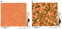
When SiC wafer is used as the substrate of RF devices, it is required that SiC should be semi insulating and its resistivity should be greater than 10 ^ 6 Ω· cm. In fact, the resistivity of silicon carbide should be very high, but [...]
2020-08-25meta-author
New research of SiC and GaN technology along with LED technology can be shared, and we can send you paper content if you want. Please see below article title:
No.1 Technologies for Power Electronics and Packaging (SiC & GaN)
1-1.The latest development of SiC power devices
1-2.New Progress of SiC high voltage power electronic devices and applications
1-3.SiC MOSFET Device Structure and Process Study
1-4.Electro-thermal Analysis of 1.2kV-100A SiC JBS Diodes Under Current Overload
1-5.Graphene-on-SiC for gas detection and bio-sensors
1-6.Packaging of high-voltage wide-bandgap power semiconductors
1-7.High power & high temperature IGBT and WIDE bandgap power semiconductor modual package
1-8.Design and TCAD Simulation of Widegap Semiconductor Devices
1-9.GaN Power Devices Beyond 650V and 150C
1-10.High-breakdown voltage GaN HEMTs fabricated on semi-insulating GaN substrates
1-11.A Gate Driver IC for E-mode GaN HEMTs with Reverse Conduction Detection
1-12.Development of Normally-off AlGaN/GaN HFETs for Power Electronics
1-13.High crystal quality GaN-on-Si to achieve excellent isolation and dynamic performance without carbon doping
1-14.200mm/8-inch GaN power device and GaN-IC technology: a new opportunity for wafer suppliers, foundries and IDMs
1-15.200mm 40V-650V E-mode GaN-on-Si Power Technology: from Device, Package, Reliability to System
1-16.GaN, Power the Future
1-17.AlGaN/GaN heterostructure pH sensors with high Al composition in the barrier layer
1-18.In-situ Wafer Cleaning for Pre-Epitaxial Deposition for Next Generation Semiconductor Devices
No.2 Micro-LED and other Novel Display
2-1.A New Concept for Fabricating CMOS-driven, High-Performance MicroLED Displays
2-2.Study on three dimensional thermal transport in micro-LEDs at the level of kW/cm2
2-3.1 bin wavelength uniformity on 200 mm GaN-on-Si LED for micro LED application with precise strain-engineering
2-4.Integration of III-V LEDs with Silicon Thin Film Transistors for Micro-LED Displays
2-5.NAURA product solutions for Mini-LED and Micro-LED
2-6.Driving Micro LED to future Lighting and Display
2-7.Growth and fabrication of semi / non-polar LEDs and Micro-LEDs using nano-patterning technology
2-8.Imaging Light Measurement Device for Subpixel evaluation of Micro-LED and OLED Displays
2-9.China LED Display Application Industry Development Report 2018-2019
2-10.Enabling the Next Era of Display Technologies by Micro LED MOCVD Processing
2-11.Research Progress and Prospects of LED Chips for Next Generation Display Application
2-12.Influence of the Charge Transfer on the Lifetime of Quantum-Dot Light-Emitting Diodes
2-13.Low toxic quantum dots polymer nanocomposites for LED applications
2-14.Micro/Mini-LED: From Backlight to Direct-view Display
2-15.Application of COB Integrated Packaging Technology in UHD LED Display Field
2-16.Prospect analysis of the 4-in-1 technical approach in LED Display Field
2-17.Mini LED, Future Directions and Solutions – from Chipone Technology
2-18.Progress in Cooperation Between LCD and LED Industry
No.3 Technologies for Ultra-Wide Bandgap Semiconductor
3-1.An (AlxGa1-x)2O3 metal-semiconductor-metal VUV photodetector
3-2.Growth and Characterization of Ultra-Wide Bandgap Oxide Semiconductors
3-3.Progress of diamond ultra-wide-band-gap semiconductor material and devices
3-4.Application of Polycrystalline Diamond Micro-nano Powder in SiC Wafer Processing and Its Key Process Technology
3-5.Epitaxial Growth of Hexagonal Boron Nitride Films on AlN/Sapphire Templates by MOVPE
3-6.Preparation and photoelectric properties of BN films by RF-sputtering
3-7.High quality h-BN thin films and their application as flexible buffer layer for III-nitrides epitaxy
No.4 The Technology in Substrate, Epitaxy and Wafer Growth Equipment (SiC&GaN)
4-1.Synchrotron x-ray diffraction-based visualization of lattice-plane tilting of a GaN substrate and epitaxial film
4-2.In situ coherent x-ray studies of surface dynamics during OMVPE of GaN
4-3.Modeling of SiC crystal growth and epitaxy and simulation of GaN Metal Organic Vapor Deposition
4-4.The effect of n-p electrodes upon the p-type conductivity of B0.375GaN/B0.45GaN QW/QB edge emitting laser diode grown over sapphire substrate
4-5.INDUSTRY4.0 as A Major Opportunity for Electronics Processes and Products
4-6.Interrelationship Between Equipment and PVT Crystal Growth in Silicon Carbide
4-7.Advanced Chemical Concentration Control for Fabrication of Devices Using SiC
4-8.The step growth mechanism for 4H-SiC with Improved Single Polytypes
4-9.Investigation of Defect Levels of Al/Ti 4H-SiC Schottky Structures by Deep Level Transient Spectroscopy
No.5 LED Chip, Packaging, and Modules
5-1.Possible Futures for LEDs and LED Packaging
5-2.Beyond Illumination | Latest Photonics Technology, Breakthrough and Application Trend
5-3.Violet Chip Excited White LEDs for Sun-Like Lighting and Horticulture Lighting
5-4.Research and application for warm white LED of high-efficiency tri-color rare earth Phosphors by purple light Excitation
5-5.Recent progress of fluorescent materials for high-power LED
5-6.Simultaneously improve the luminous efficiency and color rendering index of GaN-based white light emitting diodes using metal localized surface plasmon resonance
5-7.Thermal Simulations of a UV LED module with nanosilver sintered die attach process on graphene coated copper substrates
5-8.Recent progress on massive transfer and integration technologies of Mini & Micro-LEDs
5-9.Anisotropic Conductive Paste and Grip Ring Direct process for mini LED die attachment
5-10.Monolithic Integrated Device of GaN Micro-LED with Graphene Transparent Electrode and Graphene Driving Transistor
5-11.GaN/Si LEDs: Towards Longer Wavelength and Smaller Current Density
5-12.Recent Advances in Achieving Ultra-High Efficiency InGaN-based LEDs
5-13.The effect of air-cavity structure on the process of vertical GaN-based light emitting diodes
5-14.A Wavelength Stabilized GaN based Laser Utilizing Distributed Bragg Reflector
No.6 RF Technology and 5G Mobile Communication
6-1.The Epi structure and Process Considerations of 6-inch GaN RF HEMT for 5G applications
6-2.High frequeny GaN HEMTs and MMICs
6-3.5G mm Wave
6-4.High-frequency GaN-on-Si transistors
6-5.Development and trend of 5G RF Devices and Circuits
6-6.High-linearity GaN HEMTs for millimeter-wave applications
6-7.A Highly Integrated Multi-Parameters RF Module for Microwave Semiconductor Testing
6-8.A Compact X-band Pallet Power Amplifier Using GaN MMIC and Discrete FETs with HMIC Technology
No.7 [...]
2019-12-02meta-author
PAM XIAMEN offers 4″ Silicon Wafer.
Diameter
Type
Dopant
Growth
method
Orientation
Resistivity
Thickness
Surface
Grade
100
N
Phos
CZ
-100
1-20
500-550
P/E/WTOx
100
N
Phos
CZ
-100
1-50
2900-3100
P/E
PRIME
100
N
Phos
CZ
-100
50-70
4850-5050
P/E
PRIME
100
N
Phos
CZ
-100
1-50
5900-6100
P/E
PRIME
100
N
Phos
CZ
-100
>10
9900-10100
P/P
PRIME
100
N
Phos
CZ
-111
1-10
4000-6000
P/E
PRIME
100
N
Phos
FZ
-111
> 20000
275-325
P/E
PRIME
100
N
Phos
FZ
-111
> 20000
275-325
P/P
PRIME
100
N
Phos
FZ
-111
2000-4000
275-325
P/P
PRIME
100
N
Phos
CZ
-111
450-500
P/P
PRIME
100
N
Phos
FZ
-111
> 20000
475-525
P/P
PRIME
100
N
As
CZ
-111
.001-.005
500-550
P/E
PRIME
100
N
Phos
CZ
-111
1-20
500-550
P/E
PRIME
100
N
Phos
FZ
-111
2000-4000
500-550
P/P
PRIME
100
N
Phos
CZ
-111
1-20
4800-5200
P/E
PRIME
100
N
Phos
CZ
-111
1-3
11300-11500
P/E
PRIME
100
N
Phos
CZ
-110
450-500
P/P
PRIME
100
N
Phos
CZ
-110
1-20
500-550
P/E
PRIME
100
P
Boron
CZ
(100)-4
0.01-0.02
175-225
P/P
PRIME
100
P
Boron
CZ
(100)-4
0.01-0.02
200-250
P/E
PRIME
100
P
Boron
CZ
(100)-4
0.01-0.02
325-375
P/P
PRIME
For more information, please visit our website: https://www.powerwaywafer.com,
send us email at sales@powerwaywafer.com and powerwaymaterial@gmail.com
Found in 1990, Xiamen Powerway Advanced Material Co., Ltd (PAM-XIAMEN) is a leading manufacturer of semiconductor material in China.PAM-XIAMEN develops advanced crystal growth [...]
2019-03-04meta-author