The minority carrier lifetime, also known as the average lifetime of non-equilibrium minority carriers, reflects the decay rate of minority carriers in semiconductor materials. It can directly reflect the quality of semiconductor materials and the performance of high-voltage high-power devices. Take the SiC bipolar power devices (eg. IGBT, PIN diode) for example.
PAM-XIAMEN can offer SiC epitaxial wafers for IGBT and PIN diodes, more specifications you can found in:
IGBT : https://www.powerwaywafer.com/sic-igbt-wafer.html
PIN diode: https://www.powerwaywafer.com/sic-on-sic-epi-wafer-for-pin-diodes.html
1. Why Minority Carrier Lifetime Is Important for SiC Bipolar Power Devices?
At present, SiC bipolar power devices, such as SiC IGBTs and SiC PiN diodes, are widely used in high-voltage and high-power fields. For high-voltage and high-power devices, the voltage blocking layer in the device is generally very thick, and in order to perform conductivity modulation, it must have a sufficiently long minority carrier lifetime.
For example, a 15kV SiC bipolar power device requires a minimum minority carrier lifetime of 5μs, which is necessary for effective conductivity modulation. However, we not only want to achieve low conduction voltage drop in IGBT devices, but also aim to pursue higher device switching speeds and lower switching losses. Meanwhile, for SiC PiN diodes, the minority carrier lifetime in the drift region (i region) is also an important parameter that has a significant impact on the forward and switching characteristics of the diode. When the PiN diode is in forward bias, the conductivity modulation effect can reduce the conduction resistance in the drift region, forming a lower forward open state voltage.
In summary, minority carrier lifetime is a key parameter affecting the performance of SiC bipolar devices, which is of great significance for device performance improvement and design optimization.
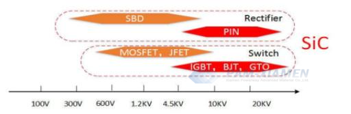
Fig. 1 Application of SiC Devices in low, medium, and high voltage fields
2. How to Enhance the Minority Carrier Lifetime of SiC IGBT Wafers?
Controlling the minority carrier lifetime of SiC epitaxial wafers needs to be considered from two aspects:
Firstly, cleanliness and operational processes should be focused to avoid the introduction of harmful impurities and reduce secondary defects induced by the process;
Secondly, reducing impurities and defects is very important, as many defects and impurities will form a center of conformity.
At present, the commonly used technical means to to enhance the lifetime of 4H SiC materials are by optimizing the epitaxial growth process, including C (carbon) or Si (silicon) ion implantation, high-temperature thermal oxidation, surface passivation treatment and etc. Through these methods, defects of SiC epitaxial wafers can be annihilated to achieve the goal of controlling minority carrier lifetime.
3. Study of Carrier Lifetime Improvement in P-Type 4H-SiC Epilayer
Researchers have found through enhancing and controlling the carrier lifetime in thick p-type 4H SiC epitaxial layers that oxidation and subsequent Ar annealing combined with appropriate surface passivation are effective in improving the carrier lifetime in p-type 4H SiC. The improvement of minority carrier lifetime in p-type 4H-SiC has been confirmed not only through thermal oxidation, but also through carbon injection and subsequent Ar annealing, such as in the case of n-type 4H-SiC. By conducting thermal oxidation for 45 hours at 1350 ℃ and followed by Ar annealing for 30 minutes at 1550 ℃, the minority carrier lifetime in p-type SiC can be increased from 0.9us (during growth) to 2.6us. However, the improvement is not as significant as in n-type SiC. It’s speculated that the insufficient elimination of Z1/2 center may be the reason for the less improvement in the lifetime of p-type epitaxial layers, which requires further experiment and analysis.
In addition, the carrier lifetime in p-type 4H-SiC can be improved from 0.1us to 1.6us by using lifetime enhanced epitaxial layers and electron irradiation with 200keV or 400keV irradiation energy. The uniform distribution of carrier lifetime within the irradiation area has been confirmed through lifetime mapping.

For more information, please contact us email at victorchan@powerwaywafer.com and powerwaymaterial@gmail.com.