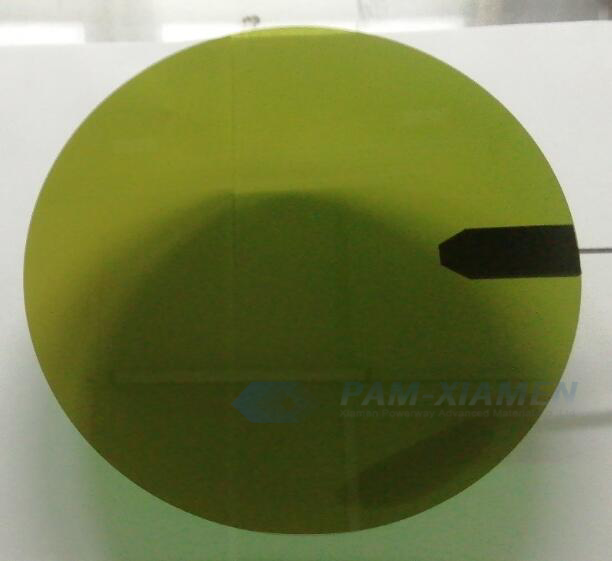
Silicon carbide (SiC) single crystals are at the forefront of the silicon carbide industry chain, and are the foundation and key to the development of the high-end chip industry. The larger the SiC substrate size, the more chips can be manufactured on per unit substrate, and the smaller the edge waste, so the lower the unit chip cost. The 8-inch SiC substrate will have a significant cost reduction advantage over the 6-inch SiC substrate. 200mm wafers for sale of 4H-SiC from PAM-XIAMEN, a leading semiconductor wafer vendor, are provided with the following specific parameters:
1. Specification of SiC 200mm Wafers
|
8 Inch N-type SiC Substrate |
|||
| Item | A Grade | B Grade | C Grade |
| Diameter | 200±0.2mm | ||
| Thickness | 500±25μm | ||
| Polytype | 4H | ||
| Surface Orientation | 4°toward <11-20>±0.5º | ||
| Dopant | n type Nitrogen | ||
| Notch Orientation | [1-100]±5° | ||
| Notch Depth | 1~1.5mm | ||
| Resistivity | 0.015~0.025 ohm·cm | 0.01~0.03 ohm·cm | NA |
| LTV | ≤5μm(10mm*10mm) | ≤10μm(10mm*10mm) | ≤15μm(10mm*10mm) |
| TTV | ≤10μm | ≤15μm | ≤20μm |
| BOW | -25μm~25μm | -45μm~45μm | -65μm~65μm |
| Warp | ≤35μm | ≤50μm | ≤70μm |
| Micropipe Density | ≤2ea/cm2 | ≤10ea/cm2 | ≤50ea/cm2 |
| Metal Content | ≤1E11 atoms/cm2 | ≤1E11 atoms/cm2 | NA |
| TSD | ≤500ea/cm2 | ≤1000ea/cm2 | NA |
| BPD | ≤2000ea/cm2 | ≤5000ea/cm2 | NA |
| TED | ≤7000ea/cm2 | ≤10000ea/cm2 | NA |
| Surface Roughness(Si-face) | Ra≤0.2nm | Ra≤0.2nm | Ra≤0.2nm |
| Front Surface Finished | Si-face CMP | ||
| Particle | ≤100(size≥0.3μm) | NA | NA |
| Scratches | ≤5,Total Length≤Diameter | NA | NA |
| Edge chips/indents/cracks/stains/ contamination |
None | None | NA |
| Polytype Areas | None | ≤20% (Cumulative area) | ≤30% (Cumulative area) |
| Front Marking | None | ||
| Back Surface Finished | C-face polished | ||
| Scratches | NA | NA | NA |
| Back defects edge chips/indents | None | None | NA |
| Back Roughness | Ra≤5nm | Ra≤5nm | Ra≤5nm |
| Back Marking | Notch(the right side) | ||
| Edge | Chamfer | Chamfer | Chamfer |
| Packaging | Epi-ready with vacuum packaging; Multi-wafer or Single wafer cassette packaging | ||
Notes: “NA”means no request. Items not mentioned may refer to SEMI-STD.
2. What Are the Difficulties and Corresponding Solutions for 200mm Silicon Carbide Wafer Preparation?
The current difficulties in the preparation of 200mm 4H-SiC crystals mainly involve:
1) The preparation of high-quality 200mm 4H-SiC seed crystals;
2) Large size temperature field non-uniformity and nucleation process control;
3) The transport efficiency and evolution of gaseous components in large size crystal growth systems;
4) Crystal cracking and defect proliferation caused by large size thermal stress increase.
To overcome these challenges and obtain high quality 200mm SiC wafers,solutions are proposed:
In terms of 200mm seed crystal preparation, appropriate temperature field, flow field, and expanding assembly were studied and designed to take into account crystal quality and expanding size; Starting with a 150mm SiC seed crystal, carry out seed crystal iteration to gradually expand the SiC crystal size until it reaches 200mm; Through multiple crystal growth and processing, gradually optimize the crystal quality in the crystal expanding area, and improve the quality of 200mm seed crystals.
In terms of 200mm conductive crystal and substrate preparation, research has optimized the temperature field and flow field design for large size crystal growth, conduct 200mm conductive SiC crystal growth, and control doping uniformity. After rough processing and shaping of the crystal, an 8-inch electrically conductive 4H-SiC ingot with a standard diameter was obtained. After cutting, grinding, polishing, processing to obtain SiC 200mm wafers with a thickness of 525um or so.

For more information, please contact us email at victorchan@powerwaywafer.com and powerwaymaterial@gmail.com.