
850nm VCSEL Array Chip with 21 Emitters for Short Distance Detection
850nm VCSEL array chip with 21 emitters can be offered. This chip is mainly used in smart homes (tablet computers, sweeping robots), distance measurement of the rear camera of mobile phones (1D ToF), and short distance detection of smart machines, etc. More details please refer to the followings:
1. 850nm VCSEL Array Product Description & Features
Item No. PAM850V021K
· 850nm VCSEL Array
· 175-215mW @ 200mA
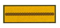
Number of emitters: 21
2. Mechanical Characteristics of 850nm VCSEL Array
| Number of emitters | 21 |
| Chip width | 260±20um |
| Chip length | 680±20um |
| Chip height | 100±10um |
| Emission pitch | 28.5um |
3. Electro-Optical Characteristicsof 850nm VCSEL Array Chip with 21 Emitters
| Parameters | Symbol | Min | Typical | Max | Units | Test Condition |
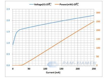
| Threshold current | Ith | – | 30 | – | mA | 25℃, @200mA, CW mode |
| Operating voltage | Vf | 1.90 | 2.10 | 2.30 | V | |
| Wavelength | λpeak | 845 | 850 | 855 | nm | |
| Output optical power | P | 175 | 190 | 215 | mW | |
| Slope efficiency | ηs | – | 1 | – | W/A | |
| Power conversion efficiency | PCE | 40 | 43 | – | % | |
| Beam full divergence (D86) | φ | 20 | 25 | 30 | ||
| Wavelength Temp. coefficient | dλ/dT | 0.07 | nm/℃ |
4. 850nm VCSEL Array Typical Performance Curves at 25℃
5. Absolute Maximum Ratings of 850nm VCSEL Array with 21 Emitters
| Parameters | Conditions |
| Forward DC current | <300mA |
| Storage temperature | -40 to 85℃ |
| Packaging temperature | ≤260℃(<10S) |
| Junction temperature | ≤120℃ |
6. Bandwidth Limiting Factors for High-Speed VCSEL
High speed VCSEL has three main bandwidth limiting factors: parasitic capacitance limitation, damping limitation, and thermal effect limitation. To achieve high modulation bandwidth, it is necessary to reduce these three limiting factors.
In response to parasitic effects, efforts should be made to reduce the resistance and capacitance of VCSEL devices as much as possible. The methods used include optimizing the conduction and valence band interfaces and doping content in DBR, using low dielectric constant thick polymer insulation material as support under the signal pad, introducing multiple deep oxide layers, and proton injection technology.
To reduce damping limitations, there are two optimization methods for high-speed VCSEL: using strain quantum wells and using half wavelength cavities and small oxide apertures.
The thermal effect is alleviated by reducing the series resistance of VCSEL, using high thermal conductivity DBR, and using copper plated heat sinks.
In recent years, research reports have shown that the modulation bandwidth is generally around 30GHz, and after optimization, it can approach 35GHz, which is considered the limit of conventional oxide limited VCSEL. The traditional short-range optical interconnect technology directly modulates and detects VCSEL and MMF through a non return to zero (NRZ) modulation scheme, suitable for 25Gbs fiber optic links. However, with the growth of data traffic, it is necessary to develop higher modulation rate links, and the improvement of modulation rate depends on the technological progress of modulation methods and electronic driving devices. To improve the modulation rate, various new technologies need to be introduced, including Digital Signal Processing (DSP), WDM, Forward Error Correction (FFC), pulse shaping, etc. New modulation methods also need to be introduced, such as Four level pulse amplitude modulation (PAM4), Carrier free amplitude/phase modulation (CAP), Discrete multi tone modulation (DMT), etc.

For more information, please contact us email at [email protected] and [email protected].