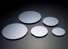
PAM-XIAMEN can offer 4” GaAs HEMT epi wafer with 2D electron gas (2DEG) and very high electron mobility of 5-7E5 cm2/V.s, please see below typical wafers of gallium arsenide with HEMT structure:

1. GaAs HEMT Epitaxial Wafer Structures
Structure 1: 4″ AlGaAs / GaAs HEMT epi wafer (PAM200416-HEMT):
| HEMT structure | Thickness |
| GaAs cap layer | 100A |
| AlGaAs, x=0.28,barrier layer, Si doped 7E17 | 500A |
| AlGaAs, x=0.28,spacer layer | 150A |
| GaAs | 0.5um |
| AlxGaAs/GaAs, x=0.28, SL | 30A/30A, 10 period |
| GaAs buffer | 2000A |
| GaAs substrate | — |
300K,Mobility :> 5000cm2/V.s, Ns>4.0E11
77K, Mobility: > 150,000-190,000 cm2/V.s,Ns>4.0E11
Structure 2: GaAs MBE epiwafers
1) 4″ SI substrate GaAs with [100] orientation,
2) [buffer] superlattice of Al(0.3)Ga(0.7)As/GaAs with thicknesses
10/3 nm, repeat 170 times,
3) barrier Al(0.3)Ga(0.7)As 400 nm,
4) quantum well GaAs 20 nm,
5) spacer Al(0.3)Ga(0.7)As 15 nm,
6) delta-doping with Si to create electron density 5-6*10^11 cm^(-2),
7) barrier Al(0.3)Ga(0.7)As 180 nm,
8) cap layer GaAs 15nm.
It can be to design nano-electronic devices by depositing metallic gates above the 2DEG on GaAs HEMT wafer to study quantum physics at ultra-low temperatures.
Structure 3: GaAs HEMT epi wafer (PAM-190125-GAAS-HEMT)
| Layer | Composition | Thickness(nm) |
| Cap | GaAs | 10 |
| Doping carrier | Al0.28GaAs1-0.28: Si 1.4*1018cm-3 | – |
| Spacer | Al0.28GaAs1-0.28 | 18 |
| Channel | GaAs | – |
| SL | GaAs/Al0.28GaAs1-0.28 24A*24A | – |
| Buffer | GaAs | – |
| Substrate | SI GaAs(100), 4” | – |
Structure 4: GaAs 2DEG Epiwafer (PAM190311-HEMT)
Mobility: 1.5e6 cm2/Vs
Carrier concentration: 3e11/cm2
| Layer Name | Material | Thickness(nm) |
| Cap | GaAs | 17 |
| Doping carrier | Al0.33Ga0.67As:Si | – |
| Spacer | Al0.33Ga0.67As (undoped) | 80 |
| Channel | GaAs | – |
| SL | (GaAs-Al0.33Ga0.67As)*100 | – |
| Buffer | GaAs | – |
| Sub | SI GaAs(100) | 500000 |
2. Measuring Thickness of GaAs HEMT Epi Wafer by Infrared Interference
This method is suitable for the measurement of the GaAs HEMT epitaxial layer thickness, and the measured thickness is greater than 2 um. The resistivity of the GaAs substrate material is required to be less than 0.02 ohm-cm, and the resistivity of the epitaxial layer is greater than 0.1 ohm-cm.
The optical constants of the gallium arsenide substrate material and the epitaxial layer are quite different. When the infrared light hits the surface of the GaAs HEMT epitaxy, interference fringes are generated in the reflection spectrum. The thickness of the epitaxial layer can be calculated according to the maximum or minimum wavelength position of the interference fringe, the optical constant of the substrate material and the epitaxial layer, and the beam angle.
The instrument for testing the epitaxial wafer of GaAs HEMT should be dual-beam infrared spectrophotometer or Fourier infrared spectrometer, the wavelength range is 2.5 um~50 um, or the wavenumber range is 4 000 cm-1~200 cm-1.
The wavelength and wavelength repeatability error of the instrument is not more than 0.05 um, and the spectral resolution at 10 um is 0.02 um or better.
The instrument should be equipped with reflective accessories, and the angle of fire should not be greater than 30°. Moreover, the instrument should be equipped with a diaphragm of various apertures made of black body material.
The sample of gallium arsenide epitaxy wafer for HEMT device used for measurement should have a good optical surface and should not have a large area of passivation layer.
The conductivity type of the substrate, the epitaxial layer and the resistivity of the substrate should be known.
3. FAQ About GaAs HEMT Epi
Q1: Would you please let me know the possible operating frequencies of the GaAs HEMT Epi wafer listed below?
1) 4″ SI substrate GaAs with [100] orientation,
2) [buffer] superlattice of Al(0.3)Ga(0.7)As/GaAs with thicknesses 10/3 nm, repeat 170 times,
3) barrier Al(0.3)Ga(0.7)As 400 nm,
4) quantum well GaAs 20 nm,
5) spacer Al(0.3)Ga(0.7)As 15 nm,
6) delta-doping with Si to create electron density 5-6*10^11 cm^(-2),
7) barrier Al(0.3)Ga(0.7)As 80 nm,
8) cap layer GaAs 15nm.
A: We always use Quantum well InGaAs in fourth layer structure, which PHEMT products, if you use 0.25 micron technology and 30GHz module circuit, or 0.07um process and 80-120GHz. Of course your art technology level and level of circuit design would be also a factor.
Q2: As for AlGaAs HEMT wafer samples, we have no strict requirements for the thickness of each layer of material. We are concerned that at low temperature (4.2K), the mobility of two-dimensional electrons in the material should be better than 1.5e6 cm2/Vs, and the carrier concentration should be about 3e11/cm2. Unlike HEMT, we hope that the top layer of the sample is not conductive, so that we can use the gate voltage to modulate the carrier concentration of the two-dimensional electron layer to make structures like quantum dots. So, could you please tell me the mobility and carrier concentration of AlGaAs/GaAs HEMT epiwafer sample you can provide?
A: The carrier concentration of GaAs HEMT epiwafer we provide can meet 3E11/cm2. At 4.2K, the mobility can be garanteed at 5-7E5 cm2/V.s, and carrier concentration at 3-4E11/cm2.
For more information, please contact us email at victorchan@powerwaywafer.com and powerwaymaterial@gmail.com.

