PAM-XIAMEN supplies GaN HEMT epitaxial wafers and GaN fabrication services. Our GaN fabrication services supplied include front-end process and back-end process. More details about GaN fabrication process for HEMTs please see below:
1. OEM Service – Si-based GaN Epitaxial Wafers for Power and RF Electronic Devices
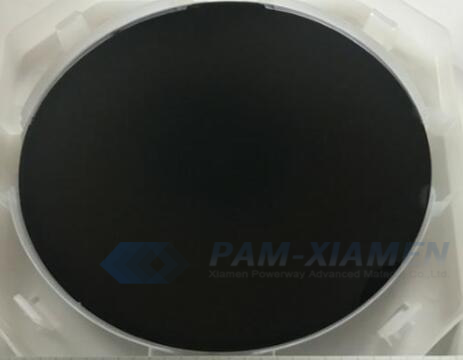
Our GaN fab can epitaxy 4-8 inch GaN wafers, which is suitable for power, RF electronic devices according to your structural requirements OEM.
2. GaN Chip Foundry Service for Power and RF Devices
We can supply photolithography, reactive ion etching, reactive ion etching (SiO2, Si3N4), PECVD (SiO2, Si3N4), electron beam evaporation (Au, Ni, Cr, Al, Ti), electron beam evaporation (ITO), rapid annealing, CMP (thinning, grinding, polishing) and etc services for GaN fabrication process of HEMT devices.
2.1 Photolithography
We can accurately control the photolithography with 1μm for the GaN wafers in sizes of 4 inch and below. Also we can perform precisely photolithography based on your demands.
2.2 Inductively Coupled Plasma Etching (ICP)
We can do pattern etching for GaN, AlN and AlGaN materials.
2.3 Reactive Ion Etching (RIE)
We can deposit SiO2 and SiNx thin films on GaN HEMT wafers by pattern etching.
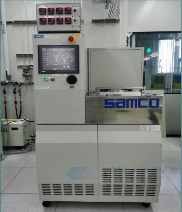
2.4 Plasma Enhanced Chemical Vapor Deposition (PECVD)
We can epitaxy a uniform, dense, and thickness-controllable SiO2 or SiNx film on the surface of GaN HEMT epi of 6 inch and below by Plasma-enhanced chemical vapor deposition.
2.5 Electron beam evaporation coating (E-Beam)
The target material is bombarded by the electron beam of the electron gun, and the ITO film (Au, Ni, Cr, Al, Ti, etc) is evaporated on the GaN surface.
Or do vapor deposition of metal films such as Ag and Pt.
2.6 Rapid Annealing (RTA)
We can do rapid annealing based on your needs, choosing gases like N2 and O2 to match your process requirement.
At the moment, in order to achieve the electrical requirements of the GaN devices you need, we will set different heating and cooling rates, annealing temperatures and times to alloy and fuse the metal electrodes.
3. GaN Test Service
We supply test services for GaN epitaxial wafers to ensure the quality of GaN fabrication process, which are:
3.1 XRD Test of Semiconductor Thin Film Materials
We use ω-scanning to scan different crystal planes of 2-4 inch GaN thin film HEMT materials. Based on the inversion space imaging principle of the rocking curve test, we will achieve inversion space mapping measurement, get the composition and stress of AlGaN, and measure of film thickness.
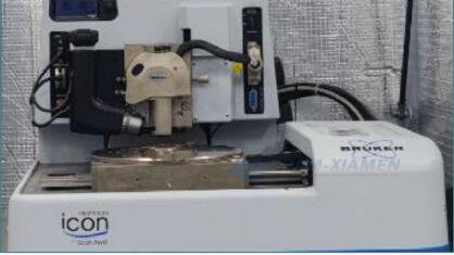
3.2 AFM Test for Epiwafers
There are 2 modes for AFM test: one is tapping and another is contact. AFM equipped with a C-AFM module can detect the surface topography of GaN and also can probe current channels in GaN.
The work function of metal materials and surface potential of GaN semiconductor can be tested by KPFM. While the friction force of the micro-domains on GaN epi can be measured by LFM function. For magnetic domain distribution, we can use MFM function to test.
3.3 Epitaxial Wafer PL Spectrum Scanning Imager
Our epitaxial wafer PL spectrum scanning imager in the foundry can test semiconductor wafers under size of 6 inch.
The test content include epitaxial film thickness and reflectivity (PR); display and output the average value of each measured parameter (Mean), mean square error (Std), standard deviation rate (CV) and etc. In addition, the test can show the mapping distribution of each parameter and the warp of the wafers.
3.4 Kelvin Probe Force Microscope
The atomic force microscope has the test function of KPFM. It can measure the work function of metal materials and the surface potential of GaN HEMT wafers. It can test the changes of surface potential of HEMT devices under illumination when installed with a light-assisted test system.
3.5 High and Low Temperature Hall Effect Test
High temperature Hall measurement of semiconductor thin film materials is available. The test temperature is 90-700K, and the magnetic field strength of the magnet is 0.5 T, the maximum measured sheet resistance is 10^11 ohm/sq, the minimum test current is 1μA, the DC range is from 1μA to 20 mA, and AC mode is also available (high resistance samples cannot be measured in AC mode).
3.6 Deep Level Transient Spectrum
We supply high-temperature deep-level transient spectroscopy and light-assisted deep-level transient spectroscopy testing, which can detect semiconductors Deep energy levels and interface states of medium and trace impurities and defects. The deep level transient spectrum can be given to characterize the semiconductor band gap The DLTS spectra of impurities, deep defect levels and interface states within the distribution with temperature.
3.7 Quantum Transport Test
We have low temperature and strong magnetic field quantum transport test, Line magneto resistance test and Hall test. The samples are First measure the variable temperature IV, and then measure the magneto resistance. Magneto-resistive measuring range is 0.1ohm-100ohm.
For III-V semiconductors, sample mobility and electron concentration changes with temperature can be tested by low temperature and strong magnetic field Hall measurement.
For quantity samples of sub-confinement effects such as two-dimensional electron gas, low warm and strong magnetic fields can lead to Zeeman splitting, so quantum effects such as SdH oscillations can be measured, and transport properties of different subbands (mobility electron concentration Spend) can be obtained.
3.8 Analysis of Electrical Parameters of Semiconductor Thin Film Materials and Structures
Electrical parameter analysis of semiconductor thin film materials and structures is provided. We analyze it based on following electrical parameter
DC source measurement unit indicators: maximum voltage 210V, maximum current 100mA, maximum power 2W; pulse measurement unit indicators: system pulse generator frequency: 50MHz-1Hz; minimum pulse width: 10ns; maximum pulse voltage: 80V, -40V-40V.
3.9 Tip Enhanced Raman Spectrometer
We can do micro-area Raman testing, possess Neaspec tip-enhanced Raman spectrometer (TERS), with a spatial resolution of 10nm, and increased Raman intensity.
The test equipment is more than 1000 times stronger, and can measure the near field strength and bit confidence of the third order or more.
Remark:
The Chinese government has announced new limits on the exportation of Gallium materials (such as GaAs, GaN, Ga2O3, GaP, InGaAs, and GaSb) and Germanium materials used to make semiconductor chips. Starting from August 1, 2023, exporting these materials is only allowed if we obtains a license from the Chinese Ministry of Commerce. Hope for your understanding and cooperation!

For more information, please contact us email at victorchan@powerwaywafer.com and powerwaymaterial@gmail.com.