Pure silicon is more like an insulator than a conductor, and when external forces are applied (such as applied voltage), it has no ability to change its conductive state. So other elements must be doped into silicon, and the two most important dopants are boron (B) and phosphorus (P). PAM-XIAMEN can supply CZ grown highly boron-doped silicon wafers for fabricating GaN power device. The specification of highly doped silicon wafer is attached for your reference, and additional CZ wafer specifications please refer to https://www.powerwaywafer.com/silicon-wafer/cz-mono-crystalline-silicon.html.
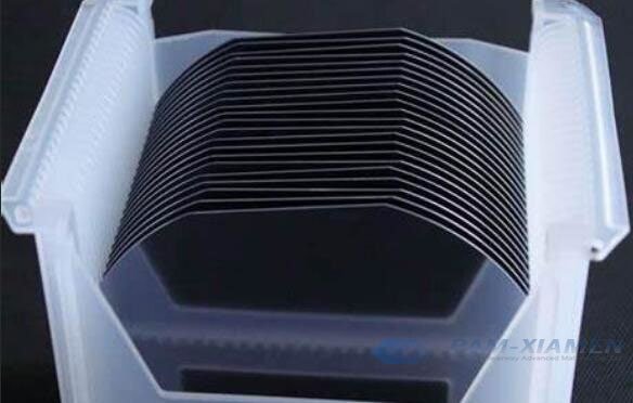
1. Specification of Highly Doped Silicon Substrate for GaN Power Device
PAMP22439 – CZS
| Item | Silicon substrate |
| Growth Method | CZ |
| Diameter | 200±0.2mm |
| Thickness | / |
| Conductivity Type | P++ |
| Crystal Orientation | (111)±0.5° |
| Dopant | Boron |
| Resistivity | / |
| GBIR (Global Flatness) | ≤5um |
| Warp | / |
| Bow | / |
| Flatness SFQR (22*22mm) | ≤0.8um |
| GBIR (TTV) | ≤5um |
| Particle (LPD) | / |
| Surface Finish | Polished (SSP) |
| Backside Condition | Etched |
| Edge | Semi-standard |
| Notch | <110> semi-standard |
2. What Are the Differences of Heavy Doping and Light Doping in Silicon?
According to the doping concentration, the doping pf semiconductor silicon wafers can be divided into light doping and heavy doping. And the differences of lightly doped Si wafer and heavily doped Si wafer are:
- Lightly doped silicon wafers have low doping concentration and are generally used in the field of integrated circuits, with higher technical difficulties and product quality requirements. Light doped silicon wafers can improve the integrity of CMOS gate oxide layers, improve channel leakage, and improve the reliability of integrated circuits by growing high-quality epitaxial layers.
- The heavily doped silicon wafers have a large amount of doped elements; highly doped silicon resistivity is low. The highly doped silicon substrates are generally used in power devices, such as GaN power devices. The power device combines the characteristics of heavily doped substrates and epitaxial layers, ensuring the reverse breakdown voltage of the device while effectively reducing the forward power consumption of the device.
3. Why Use Boron as Electroactive Impurity for P-Type Silicon?
B is the most important electroactive impurity in p-type monocrystalline silicon for the following reasons:
1) Introducing B atoms, holes will be generated inside the Si crystal, and the number of holes increases with the increase of B atom concentration;
2) The IIIA group elements B, Al, Ga, and In all belong to acceptor impurities and can provide holes for Si crystals. However, due to the small segregation coefficients of AI, Ga, and In, it is difficult to control the crystal resistivity during doping when used them as dopants. However, the segregation coefficient of B in Si is about 0.8, which is close to 1, resulting in good consistency in the resistivity of the first and last silicon wafers of B-doped single crystal silicon, improving the utilization rate of the entire single crystal.
3) At room temperature, B has a large solid solubility (2.2X 10²⁰/cm3) in single crystal Si. Therefore, the controllable range of the resistivity of p-type Si materials is large by adjusting the concentration of B, with a minimum resistivity of 0.1m Ω·cm-1;
4) The increase in oxygen concentration in the highly doped silicon wafers enhances oxygen precipitation, thereby improving the internal impurity absorption ability of silicon wafers;
5) Heavy doping of B can improve the mechanical strength of silicon wafers and suppress void defects.

For more information, please contact us email at victorchan@powerwaywafer.com and powerwaymaterial@gmail.com.