The silicon carbide crystal most commonly used as a semiconductor material is 4H-SiC wafer. However, silicon carbide crystals have multiple types. Once the conditions are not well controlled in the process of the silicon carbide crystal growth, the resulting silicon carbide crystal structure may be 3C, 6H, 15R, etc., but not 4H.
Two aspects should be considered in the growth of silicon carbide crystal:
- The growth characteristics of the SiC crystal itself. The main growth characteristic is the phase transition point, including melting point and decomposition point. An appropriate crystal growth method should be selected based on its growth characteristics. As for the large silicon carbide crystalgrowth, the common methods are the liquid phase method with solid-liquid phase change and the gas phase method with solid-gas phase change, which are classified by the phase sate, participated in the process. Generally, the solid phase method is not used in the silicon carbide growth process, for the shortcomings of pure solid-solid phase transformation are difficult to overcome.
- The conditions that the equipment can withstand. If the conditions are not met, it is impossible to grow. Moreover, industrialized production has to consider cost.
The characteristics of silicon carbide crystals can be analyzed on the basis of the phase diagram (Changes in temperature and other conditions of the draw is not very accurate):

Under normal conditions, silicon carbide has decomposed before it becomes a liquid, so there is no pure silicon carbide in a liquid state participating in the SiC crystal growth process. If Si is excessive, the liquid phase range is 0.01%~19%, and it is possible to use the liquid phase method. However, when the temperature is higher than 1700℃, large amount of Si will evaporate, thus, the SiC crystal growth cannot be achieved through simple binary eutectic growth technology.
In conclusion, the common methods for silicon carbide single crystal growth related to the liquid phase method–the uniform melting method is limited, while the non-uniform melting flux method (ternary and above, like Si-C-Cr) is still under development. The liquid phase method has four major advantages:
- Diameter expansion;
- Thicken;
- Capable of P-type doping;
- The dislocation density lower than the seed crystal in one magnitude.
It is funny that the sublimation-sublimation process of silicon carbide solids (2400-2500°C) can be realized at lower temperatures, which makes it possible to grow silicon carbide by sublimation. The sublimation method is a kind of gas phase method to grow silicon carbide crystal, and the gas forms crystals on the surface of a solid.
The simulation of the temperature field can be simulated by Virtual Reactor (SiC) software. The seed crystal temperature required for 4H-SiC growth is 2120-2200°C, and the air pressure is 500-3000Pa; the seed crystal temperature required for 6H-SiC silicon carbide crystal growth is 2200-2300°C, and the air pressure is 1000-10000Pa.
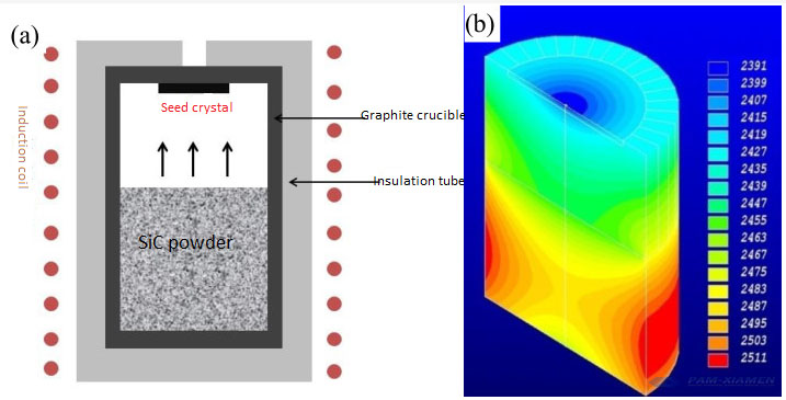
(a) PVT method for silicon carbide crystal growth
(b) The internal temperature field of SiC crystal grown by PVT method
The theoretical temperature field for growing high-purity semi-insulating 6-inch SiC: the seed crystal temperature is 2200℃, the growth pressure is 30mbar, the H2+Ar atmosphere, and the thickness can reach 22mm.
The vapor phase method grows crystals:
Whether the main process of this method is a chemical reaction can be divided into physical vapor deposition and chemical vapor deposition.
The physical vapor deposition:
The main process of this method is a physical process, and no chemical reaction occurs. The raw material gas is silicon carbide, and the growth obtained is also silicon carbide. Taking the specific equipment into account, physical vapor deposition includes sublimation-condensation (Physical Vapor Transport, PVT for short), vacuum evaporation, sputtering, ion beam deposition, molecular beam epitaxy, and laser abrasion. Law and so on.
For chemical vapor deposition (Chemical Vapor Deposition, referred to as CVD), it must involve the generation of chemical reactions. Similarly, chemical vapor deposition includes vapor phase epitaxy, hot filament method, microwave plasma chemical vapor deposition, metal organic chemical vapor deposition (MOCVD) and so on.
For example, GaAs is grown by the MOCVD method. The typical experimental method is:
The pressure is 8kPa, the temperature is 500-630°C; the raw material is the mixed gas of TMGa/AsH3 carried by H2. Under such conditions, TMGa+AsH3+H2 react to produce GaAs.
Similarly, silicon carbide can grow single crystals, using physical vapor transport and high-temperature chemical vapor deposition. As shown in the figure below, the raw material for physical vapor transport is silicon carbide solid, which turns into a gas after heating, and finally grows into a crystal on the surface of the seed crystal (note: PVT method requires a seed crystal, otherwise it is a Lely method). However, chemical vapor deposition is different. The raw material is gas, and a chemical reaction occurs directly on the surface of the seed crystal to form crystals.
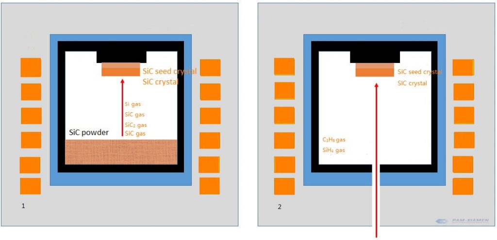
Fig. 1 PVT method of physical vapor transport
Fig. 2 High temperature chemical vapor deposition (HT-CVD) method
The crystal growth of silicon carbide by PVT method is a complex physical and chemical process. At high temperatures, the basic silicon carbide crystal growth process includes decomposition and sublimation of raw materials, mass transport, and surface crystallization of seed crystals. The growth of silicon carbide by physical vapor transport has two intrinsic properties:
- The raw material is silicon carbide solid, so the purity is not easy to control;
- In the process of turning powder into gas, a variety of gases can be generated.
The solid SiC powder will decompose and sublimate into several different gas phase components. The main gaseous components are Si, SiC, Si2C, and SiC2. The reaction formula is as below; C in the graphite crucible can react with Si vapor, generating SiC2 and Si2C; In addition, there will be a small amount of C, C2, Si2, Si3, Si2C3, etc. in the gas phase composition, but they can be ignored.
SiC(s)=Si(g)↑+C(s)
2SiC(s)=Si2C(g) ↑+C(s)
2SiC(s)=SiC2(g) ↑+Si(l,g) ↑
SiC(s)=SiC(g) ↑
C(s) +Si (l, g) =SiC(s)
During the decomposition process of SiC raw materials, due to the non-uniform sublimation of the raw materials, the number of Si atoms in the gas phase composition is far greater than the number of C atoms. A high non-stoichiometric ratio will cause the separation of Si and C. Si accumulates in the gas phase, while C aggregates in the solid phase. The growth material will be severely graphitized at the moment. Theoretically, keeping ratio of the Si: C at 1:1 near the growth interface is the most ideal growth method, but this is difficult to keep the ration in the actual silicon carbide crystal growth process. For this reason, the stoichiometric ratio can be maintained by adding an appropriate amount of Si to the growth material to balance the excess C.
When Si, SiC, Si2C, SiC2 gases reach the surface of the seed crystal, crystals are continuously formed in the metastable region:
SiC (g) =SiC(s)
Si (g) +SiC2 (g) =2SiC(s)
Si2C (g) +SiC2 (g) =3SiC(s)
Therefore, the defects of the grown silicon carbide single crystal need more technical means to control and it is generally used to produce conductive SiC substrates.
The chemical vapor deposition method uses special gases as raw materials, making a higher cost. Now, it can only be used to produce semi-insulating SiC substrates. The two typical chemical reaction paths are as follows:
C2H (g) + 2SiH4 (g) — 2SiC(s) + 6H2 (g)
3SiH4 (g) + C3H8 (g) — 3SiC(s) + 10H2(g)
Only using SiH4, Si droplets will be formed when V (Si): V (H2)>0.05%. Then, halogens can be introduced into the raw materials, which can reduce Si defects. The types used include HCl, SiCl4, SiHCl3, CH3Cl, SiCl3H3, and SiH3Cl.
The required equipment can be the horizontal hot wall CVD-VP508, including deliberate doping growth zone, unintentional doping growth zone, heating system, cooling system, vacuum system, gas supply system, exhaust gas treatment system, control system and alarm system.
The silicon carbide crystal growth procedure includes cleaning the substrate (seed crystal), etching under vacuum, and then epitaxial growth:
Substrate preparation and cleaning——Put the substrate into the reaction chamber——Vacuum——High temperature in-situ etching of the substrate——Inject the original gas for the epitaxial growth of SiC——The experiment is over, take out the sample
Growth rate: 5-10um/h, the standard process is as follows:
- Si source: SiH4SiHCl3 SiCl4
- C source: CH4C2H6 C3H8 CCl4
- Carrier gas: H2, Ar
- Temperature: 1200-1800℃
- Air pressure: 10-1000mbar
PS: 1bar=1atm=100kPa, easy to compare with the standard atmospheric pressure
This is the main method for silicon carbide crystal growth, the two vapor phase methods: PVT method and HTCVD method.

For more information, please contact us email at victorchan@powerwaywafer.com and powerwaymaterial@gmail.com.