Epitaxial GaN template grown on Al2O3 (sapphire) substrate and customizable stacks are available with high quality and low defect density. Attached are a list of several types of GaN thin film on sapphire substrate wafers with different thicknesses, carrier types, and capping layers that we manufactured:
1. Specifications of GaN Thin Film Epitaxy PAM160107-GAN
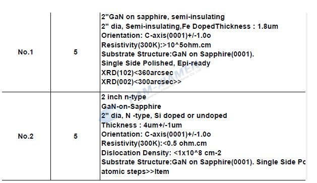
No.1 Epitaxial GaN on Sapphire Substrate
| Layer | Material | Thickness | Doping |
| 2 | GaN | 5 µm | – |
| 1 | C doped-GaN Buffer | – | 5E18-1E19 |
| Sapphire substrate |
Remark: the thickness tolerance is 4um +/-1um, and carrier concentration should be <3E17 (not doping concentration, because it is undoped). If you want carrier concentration <1016, we can do it, but we need to adjust production, which lead to higher cost.
No.2 Epitaxial GaN on Al2O3 Substrate
| Layer | Material | Thickness | Doping |
| 2 | GaN | – | n- < 1017cm-3 |
| 1 | U-GaN Buffer | 1-2 µm | – |
| Sapphire substrate |
Remark: The regular carrier concentration should be (5-8) E16 (not doping concentration). And we cannot change the carrier concentration.
No.3 GaN Epilayers on Sapphire
| Layer | Material | Thickness | Doping |
| 4 | GaN | – | p+ 1019 cm-3 Mg |
| 3 | GaN | 5 µm | – |
| 2 | GaN | – | N+ 1019 cm-3 |
| 1 | U-GaN Buffer | 1-2 µm | – |
| Sapphire substrate |
No.4 Single-Crystal GaN on Sapphire
| Layer | Material | Thickness | Doping |
| 3 | GaN | – | n- < 1016 cm-3 |
| 2 | GaN | 1 µm | – |
| 1 | U-GaN Buffer | 1-2 µm | – |
| Sapphire substrate |
No.5 GaN Thin Film on Sapphire
| Layer | Material | Thickness | Doping |
| 4 | AlN | – | UID |
| 3 | GaN | – | n- < 1016 cm-3 |
| 2 | GaN | 1 µm | – |
| 1 | U-GaN Buffer | 1-2 µm | – |
| Sapphire substrate |
No.6 Sapphire based GaN Template
| Layer | Material | Thickness | Doping |
| 3 | AlN | – | UID |
| 2 | GaN | 0.250 µm | – |
| 1 | C doped-GaN Buffer | 1-2 µm | 5E18-1E19 |
| Sapphire substrate |
Remark: For the GaN template wafers from No.3 to No.6, we can achieve carrier densities <10E16 cm-3 in specific different layers.
No.7 Gallium Nitride Thin Films Grown on Sapphire Substrate
| Layer | Material | Thickness | Doping |
| 4 | GaN | – | p+ 1019 cm-3 Mg |
| 3 | GaN | 10 µm | – |
| 2 | GaN | – | N+ 1019 cm-3 |
| 1 | U-GaN Buffer | 1-2 µm | – |
| Sapphire substrate |
2. Buffer Layer for Growth of GaN Film on Al2O3
Will all the GaN epitaxy wafers require a 1-2 um buffer layer? For example, the wafer No.6: 100A AlN cap and 0.25um GaN, this will set directly on top of a 1-2 um buffer layer? The GaN/Sapphire wafers will all require 1 1-2um buffer layer, the precise one should be No.6: 100A AlN cap/ 0.25um GaN/buffer layer-GaN/Sapphire. Buffer layers are required for all of these GaN thin film substrate wafers due to the lattice mismatch issues between GaN and the sapphire substrate.
3. Method for Activation Anneal for GaN Film Growth
Take the activation anneal for p-type GaN thin film for example: An activation anneal following growth will not perform for the p type GaN, you can anneal 10 minutes in 830 degrees through RTA to active. And Mg doping concentration is 2E19cm3. The carrier concentration would be 4.4E17 after activation. Specifically:
For the ambient of RTA for Mg activation, the grown GaN thin film is annealed in high purity N2/O2 gas mixture and the activation of N2:O2 flow ratio is 4:1, the total volume of 5slm (standard liters per minute). The annealing temperature is 830 degrees, and the time is 10 minutes. This process is done in a rapid heating annealing furnace, not a tube type annealing furnace.
The free carrier concentration of single-crystal GaN film after activation can be measured by Hall Effect, cutting 5*5mm with metal contacts.
4. FAQ of GaN Thin Film on Sapphire
Q1: What is the doping (n-type) concentration of GaN on sapphire template and visible light transmittance could you achieve?
Is it possible to >5×10¹⁷/cm3 and visible light transmittance over 80%?
A: Doping concentration of n type GaN template on sapphire >1E20, but transmittance is below, single side polished, if double side polished, it would be better.
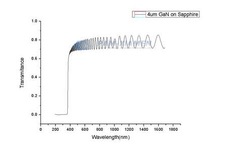
Transmitance of N-Type GaN on Sapphire
Q2: We bought these Ga-polar GaN templates while ago as below. I was wondering if you can provide me with the GaN crystal direction with respect to the flat on substrate. Is the flat in GaN a-direction or m-direction?
A:In No.1 GaN on Sapphire template, the flat orientation is A-plane, 16mm.
In No.2 GaN template on sapphire, the flat orientatin is M-plane, 16mm, see below:
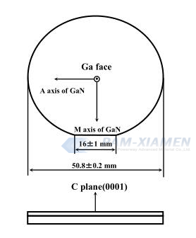
GaN Crystal Direction with Respect to the Flat on Sapphire Substrate
Q3: Currently 15 um is the max thickness of GaN thin film on sapphire that is achievable?
A: Yes, 15um thick GaN epi layer grown on sapphire is more safety.

For more information, please contact us email at victorchan@powerwaywafer.com and powerwaymaterial@gmail.com.