Monocrystalline Germanium (Ge) ingot is provided with P type by PAM-XIAMEN. Germanium crystal does not contain large-angle grain boundaries or twin crystals. It has a diamond-shaped crystal structure and is an important semiconductor material. According different applications, single crystal germanium ingot can be divided into solar-grade germanium single crystal, infrared-grade germanium single crystal and detector-grade germanium single crystal. Among them, infrared-grade Ge single crystal is used to prepare basic materials for infrared windows, infrared lenses and other optical components; Ge ingot for semiconductor devices is used to make substrate material for various transistors and solar cells; Detector-grade single crystal Ge is used to prepare high-resolution gamma radiation detector. Take the following specification for example:
1. Specification of Single Crystal Germanium Ingot
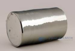
No.1 Germanium Cubic Crystal
PAM181102-GE
| Item | Germanium Cubic Crystal |
| Conduct type | S-C-P |
| Dopant | Ge-Ga |
| Length | 150 mm |
| Diameter | 100.0±0.4 mm |
| Orientation | (100)6° off Toward<111>+5° |
| Orientation Angle | 135° |
| Primary Flat | (100)+2° |
| PFlat Length | 32.5+2.5 mm |
| Secondary Flat | None |
| CC | 1E18 – 2.5 E18 |
| EPD | Ave< 500 /cm3 |
| Resistivity | 0.01-0.04 Ohm*cm |
No.2 Germanium Ingot Optical Grade
PAM200408-GE
Germanium ingot D26-0.3mm*L100mm
Germanium ingot D30-0.3mm*L100mm
Type: N-type
Orientation: <111>
Resistivity: 5-40 Ohm*cm
Absorption coefficient: 0.03cm/max @ λ= 10.6um
Refractive index heterogeneity: 5.0*10-9 max @ λ=10.6 um
2. Industry Standards for Germanium Crystal Growth
The germanium single crystal surface after spheronization should be free of cracks, holes, scratches, and the cylindrical surface should have no unrolled places.
The conductivity type of ingot type germanium should meet the requirements of Table 1:
Table 1 Conductivity Type of Monocrystalline Germanium Ingot
| Conductivity Type | Dopant | Resistivity p(23 ℃±0.5℃) ohm-cm |
| P-type | Ga | 0.001~45.0 |
| In | 0.001~45.0 | |
| Au+Ga(ln) | 0.5~5.0 | |
| N-type | Sb | 0.001~45.0 |
| Undoped | 35.0~50.0 |
The radial resistivity variation of germanium single crystal boule should meet the requirements of Table 2:
Table 2 Radial Resistivity Variation of Germanium Crystal
| Diameter (mm) | Radial Resistivity Variation (Absolute Value) |
| 10≤d≤50 | ≤10% |
| 50≤d≤100 | ≤15% |
| 100≤d≤150 | ≤20% |
| 150≤d≤200 | ≤25% |
| 200≤d≤300 | ≤30% |
| Note: The diameter refers to the size of the unrounded germanium single crystal. | |
The dislocation density of Ge ingot for different purposes should meet the requirements of Table 3:
Table 3 Dislocation Density of Germanium
| Application | Dislocation Density Pcs/cm2 |
| Semiconductor Device | ≤1 000 |
| Laser Component | ≤5 000 |
| Infrared Optical Component | ≤100000 |
Mark: The requirements for parameters of the produced pure germanium crystal will be higher than the industrial standards.
3. FAQ for Germanium Ingot
Q: What is the difference of germanium ingot between electronic grade and optical grade?
A: Optical grade germanium single crystal generally is lower requirement to electronic grade, they require transmission rate and different polished condition and orientation, but we often use low electronic grade for optical grade.

For more information, please contact us email at victorchan@powerwaywafer.com and powerwaymaterial@gmail.com.