Group III nitride materials are a kind of direct band gap materials, which have the advantages of wide band gap, strong chemical stability, high breakdown electric field and high thermal conductivity. They have broad application prospects in the fields of efficient light-emitting devices and power electronic devices. Therein, by changing the composition of In, band gap width of ternary compound InGaN materials can be continuously adjusted in the range of 1.95eV to 3.40eV, which is suitable for the active region of light emitting diodes (LED) and lasers (LD). PAM-XIAMEN is able to offer epitaxial wafer of InGaN / GaN MQW (multi quantum well) on Si substrate for fabricating laser diode with a wavelength of 405nm. Detailed specifications please refer to the table below:
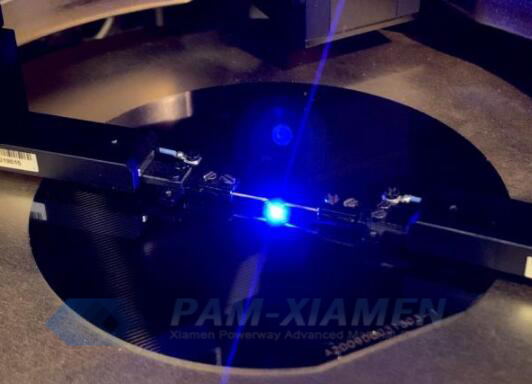
1. 405nm Violet LD Wafer Based on InGaN / GaN MQW Structure
| Epi Layer | Material | Thickness (nm) | Composition | Doping | |||
| Al% | In% | [Si] | [Mg] | ||||
| 0 | Si(111) substrate | 5.0E+18 | |||||
| 1 | nGaN | – | – | ||||
| 2 | AlGaN | – | 3-10 | – | |||
| 3 | InGaN | 70-150 | – | ||||
| 4 | MQW | InGaN-QW | – | – | |||
| GaN-QB | – | ||||||
| 5 | InGaN | – | 2-8 | ||||
| 6 | AlGaN | – | – | – | |||
| 7 | pGaN | 2.0E+19 | |||||
| 8 | Contact layer | 10 | |||||
2. Applications of High-Power Lasers Grown on InGaN / GaN Multiquantum Wells
Lasers based on GaN material systems (GaN, InGaN and AlGaN) expand the wavelength of semiconductor lasers to the visible spectrum and ultraviolet spectrum, as shown in Figure below. It has great application prospects in display, lighting, medical, national defense and security, metal processing and other fields.
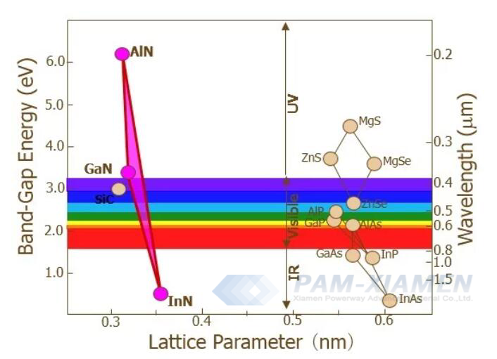
Wavelength Spectrum of GaN Materials (GaN, InGaN and AlGaN), from Visible to Ultraviolet
Among all the laser diodes, the development and application of 405 nm GaN laser have promoted the development of high-density optical storage, laser direct write lithography and light curing industries.
3. Why Epitaxial InGaN / GaN MQW Materials on Silicon Substrate?
The technology of GaN based semiconductor materials and devices on silicon substrate can not only greatly reduce the manufacturing cost of GaN based optoelectronics and electronic devices by virtue of large size, low-cost silicon wafers and their automated process lines, but also is expected to provide a new path for silicon based optoelectronic integration. Direct growth of InGaN / GaN laser diode on silicon substrate materials makes it possible for GaN based optoelectronic devices to be organically integrated with silicon based optoelectronic devices.
GaN LD wafer with blue emission is also can be supplied. For additional information, please refer to https://www.powerwaywafer.com/blue-gan-ld-wafer.html.
Remark:
The Chinese government has announced new limits on the exportation of Gallium materials (such as GaAs, GaN, Ga2O3, GaP, InGaAs, and GaSb) and Germanium materials used to make semiconductor chips. Starting from August 1, 2023, exporting these materials is only allowed if we obtains a license from the Chinese Ministry of Commerce. Hope for your understanding and cooperation!

For more information, please contact us email at victorchan@powerwaywafer.com and powerwaymaterial@gmail.com.