PAM-XIAMEN can offered SiC wafers, specific specifications and parameters can be found in: https://www.powerwaywafer.com/sic-wafer
4H-SiC single crystal has excellent characteristics such as wide bandgap, high carrier mobility, high thermal conductivity, and good stability. It has broad application prospects in high-power electronics, radio frequency/microwave electronics, and quantum information. After years of development, 6-inch 4H SiC single crystal substrates and homogeneous epitaxial thin films have been industrially applied. However, the total dislocation density in 4H SiC wafers is still as high as 103~104 cm-2, which hinders the full potential of 4H-SiC wafers. How do the dislocations affect the properties of 4H-SiC wafers and devices? The specific analysis is as follows:
1. The Effect of Dislocations on Electrical Properties in 4H-SiC Wafers and Devices
Research has analyzed the relationship between the performance of 4H-SiC wafers and devices and the distribution of dislocations within the functional region, suggesting that the presence of dislocations can have adverse effects on device performance. Therefore, studying the electrical properties of dislocations themselves is of great significance for understanding their behavior in devices.
1.1 Effect of Dislocations on Electrical Properties in 4H-SiC Substrate
By combining molten alkali corrosion and Kelvin probe force microscopy (KPFM), it can be observed that threading edge dislocation (TED) and basal plane dislocation (BPD) exhibit acceptor states in high-purity semi insulating (HPSI) 4H SiC substrates and donor states in n-type 4H SiC substrates (see Figure 1). In the 4H SiC epitaxial layer with low doping concentration, it was also found that penetrating dislocations exhibit acceptor characteristics. First principles calculations have found that TED and BPD introduce defect energy levels, with the energy level near the bottom of the valence band being the empty band. Due to the dominance of deep level defects such as impurity atoms, carbon vacancies (VC), or vacancy pairs (VC-VSi) in HPSI 4H SiC, the vacancy band introduced by dislocations can receive deep level electrons, and dislocations exhibit acceptor characteristics. In the n-type substrate, calculations show that N atoms are more stable in binding to TED and BPD dislocations, therefore N atoms tend to aggregate near dislocations. Due to the dominance of doped atoms in conductive substrates, the aggregation of N atoms can cause donor characteristics of dislocations.
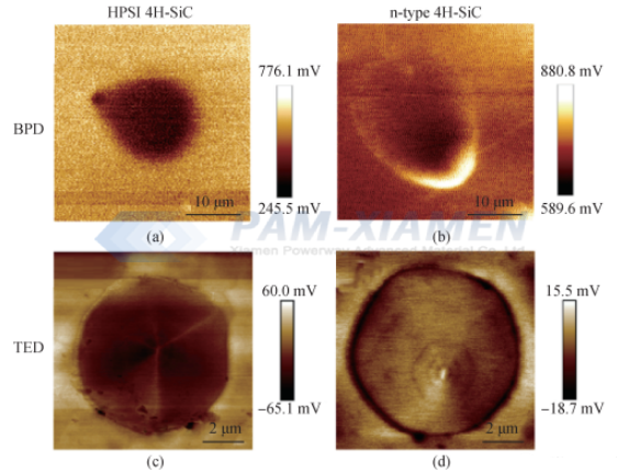
Fig. 1 Surface potential distribution of BPD and TED in HPSI and n-type 4H-SiC
1.2 Effect of Dislocations on Electrical Properties of 4H-SiC Devices
By scanning the micro pits caused by threading screw dislocation (TSD), the C-AFM test results showed a significant increase in the current at the bottom of the micro pits, while the surface current in other areas inside the micro pits was not significantly different from that outside the micro pits. This indicates that the dislocation lines of TSD in 4H SiC enhance the leakage effect. In addition, dislocations as recombination centers can cause electron hole recombination in 4H-SiC power devices and also lead to a decrease in device reliability.
Dislocation lines not only have an impact on device performance, but also cause surface micro pits at the nanoscale depth on the surface of the epitaxial layer due to the disturbance of the external step flow caused by dislocation lines. The presence of micro pits can also affect device performance. For example, under high pressure, micro plasma appears at the micro crater position caused by threading dislocation (TD), indicating that the gate oxygen at the micro crater position is first broken down. The presence of micro pits can also lead to a decrease in the lifetime of minority carriers, an increase in reverse leakage current, and a decrease in forward voltage, which have adverse effects on 4H SiC based Schottky barrier diodes (SBDs), p-n junction diodes (PNDs), and avalanche photodiodes (see Fig. 2 (a) and (b)).
Therefore, some researchers believe that the current impact of dislocations on device performance is mainly caused by micro pits, and the impact of dislocation lines themselves is secondary. Through simulation and experiments, it was found that excluding the presence of micro pits can reduce the impact of TSD on 4H-SiC based devices (see Fig. 2 (c)). BPD can also serve as a composite center in 4H-SiC. When operating in 4H-SiC bipolar devices, electrical injection can cause slip of incomplete dislocations in the silicon core, leading to stacking fault expansion and seriously affecting the forward and reverse performance of the device. It is generally believed that the stacking faults caused by incomplete dislocations in the silicon core in BPD are developed at the interface between the substrate and the epitaxial layer, and expand outward on the surface of the epitaxial layer. Considering the directional motion of two incomplete dislocations in BPD, the expansion of stacking faults caused by BPD is complex. Research has found that stacking faults caused by BPD can also move towards the interface between the substrate and epitaxial layer (see Fig. 2 (d)).
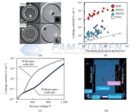
Fig. 2 The effect of dislocations on the leakage current of 4H-SiC power devices and the expansion of stacking faults in 4H-SiC: (a) EL images of avalanche diodes (left) and DIC images after melting KOH corrosion (right); (b) The relationship between leakage current of different devices and TDs density; (c) The reverse leakage behavior of 4H-SiC diodes and their dependence on nano pits; (d) EL image of 4H SiC PIN device observed by 420nm filter
2. Effect of Dislocations on Optical Properties in 4H-SiC
As a radiative recombination center, dislocations in 4H-SiC exhibit photoluminescence, and the contrast of dislocation photoluminescence (PL) depends on the lifetime of minority carriers. When the concentration of deep level defects in the crystal is low, the minority carrier lifetime is long, and enough minority carriers move to the dislocation region to recombine and emit light. At this time, the luminescence intensity of the dislocation region is higher than that of other regions, appearing as a bright spot. When the concentration of deep level defects in the crystal is high, the minority carrier lifetime is low, and it combines with nearby deep level defects to emit light. The recombination at the dislocation is suppressed, and the emission intensity in the dislocation region is weaker than in other regions, exhibiting a dark spot. The experiment found that in PL testing, for the 4H-SiC with the lifetime of minority carriers less than 0.5μs, most minority carriers cannot migrate to dislocations, and a small number of minority carriers are captured by inherent defects. Dislocations do not show significant contrast in the PL surface scan image. When the lifetime of minority carriers is greater than 0.5μs, the electron hole recombination at the dislocation can significantly distinguish the contrast of the dislocation from other regions.
TSD and TED exhibit different sizes of dark or bright spots in the PL surface scan images of 4H-SiC. The intrinsic PL emission peaks of TED and TSD are located at 600nm and 800-850nm, respectively. BPD appears as dark or bright lines in the PL surface scan image of 4H-SiC (see Fig.3 (a)). The PL emission peaks of BPDs originate from the PL emission peaks of incomplete dislocations and stacking faults that make up BPDs. The emission peaks of silicon core incomplete dislocations, carbon core incomplete dislocations, and stacking faults are located at 670-700nm, 720-850nm, and 420nm, respectively. By adjusting the wavelength of the emitted light, the display of single incomplete dislocations and stacking faults can be achieved separately.
Recently, researchers have also found that TDs can enhance the D1 luminescence of 4H-SiC, as shown in Fig.3 (b) and (c), which represent the luminescence intensity of TED and TSD corrosion pits, respectively. This means that the intensity of D1 luminescence can also reflect the density and distribution of dislocations in the 4H-SiC substrate and epitaxial layer.
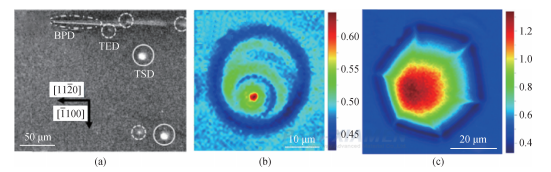
Fig. 3 Luminescent properties of dislocations in 4H-SiC: (a) Micro area PL surface scan images of 4H SiC epitaxial thin films obtained using a 900nm bandpass filter; (b) TED microregion PL surface scan images and (c) TSD microregion PL surface scan images in N-type 4H-SiC substrate obtained in the emission of 450nm~750nm.
Increasing material size and reducing dislocation density are the overall directions for the development of 4H-SiC substrates and epitaxial thin films. To reduce dislocation density, on the one hand, it is necessary to optimize the design of thermal and flow fields, design seed crystal or substrate treatment techniques, and optimize single crystal or epitaxial process technologies to reduce dislocation density; On the other hand, based on the increasingly mature process technologies, further in-depth research is needed on how to promote the transformation or reaction between different types of dislocations to reduce low dislocation density. In terms of regulating the performance of dislocations, further research is needed on how to promote the reaction between impurities and point defects with dislocations, thereby adjusting the defect energy level position and dynamic behavior of dislocations.
Reference:
Jiajun Li, Guang Yang, Xiaoshuang Liu, Hao Luo, Lingbo Xu, Yiqiang Zhang, Can Cui, Xiaodong Pi, Deren Yang and Rong Wang
Dislocations in 4H Silicon Carbide

For more information, please contact us email at victorchan@powerwaywafer.com and powerwaymaterial@gmail.com.