PAM-XIAMEN can supply SiC epitaxial wafers for MOSFET devices, additional information please read: https://www.powerwaywafer.com/sic-mosfet-structure.html. The epitaxial process of SiC inevitably forms various defects, which affect the performance and reliability of SiC power devices. Below, we specifically explore the impact of triangle defects on the performance of SiC MOSFET devices.
1. What Are Triangle Defects?
Triangle defect is a 3C-SiC polytype inclusion that extends along the basal plane direction to the surface of the SiC epitaxial layer. It may be generated by falling particles on the surface of the SiC epitaxial layer during the epitaxial growth process. The particles are embedded in the epitaxial layer and interfere with the growth process, resulting in 3C-SiC polytype inclusions that exhibit sharp triangle surface features, with the particles located at the vertices of the triangular region. Many studies also attribute the origin of polymorphic inclusions to improper parameters such as surface scratches, microtubules, and growth processes.
However, due to different growth mechanisms, there are significant differences in the morphology of many triangle defects on the surface of the epitaxial layer. It can be roughly divided into the following types:
1.1 Triangle Defect with Large Particles at the Top
This type of triangle defect has a large-sized spherical particle at the top, which may be caused by falling objects during the growth process. A small triangular area with a rough surface can be observed in the downward direction of the vertex. This is because during the epitaxial process, two different 3C-SiC layers were formed successively in the triangular region, with the first layer nucleating at the interface and growing through 4H-SiC step flow. As the thickness of the epitaxial layer increases, the second layer of 3C polytype nucleates and grows in smaller triangle pits, but the 4H growth step does not fully cover the 3C polytype area, making the V-shaped groove area of 3C-SiC still clearly visible, shown as in Fig 1.
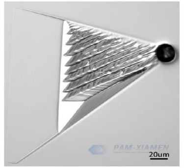
Fig. 1 Surface morphology of triangle defects with large particles at the top
1.2 Small Particles at the Top and Rough Triangle Defects on the Surface
The particles at the vertices of this type of triangle defect are much smaller, as shown in Fig. 2. And most of the triangular regions are covered by the step flow of 4H-SiC, that is, the entire 3C-SiC layer is completely embedded below the 4H-SiC layer. The triangle defect surface can only see the growth steps of 4H SiC, but these steps are much larger than the conventional 4H crystal growth steps.
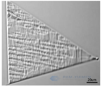
Fig. 2 Diagram of small particles at the top and rough triangle defects on the surface
1.3 Smooth Triangle Defects on the Surface
This type of triangle defect has a smooth surface morphology, as shown in Fig. 3. For such triangle defects, the 3C-SiC layer is covered by step flow of 4H-SiC, and the surface 4H crystal growth is finer and smoother.
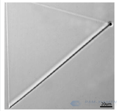
Fig. 3 Surface morphology of smooth triangle defects on the surface
2. Influences of Triangle Defects on the Characteristics of SiC MOSFET Devices
Researchers have studied the influences of triangle defects on SiC MOSFET performance, and the results are show as Fig. 4, which shows a histogram of the statistical distribution of five characteristics of devices with triangle defects. The blue dashed line represents the segmentation line of device degradation, and the red dashed line represents the segmentation line of device failure. For device failure shown as in Table 1, triangle defects have a significant impact, with a failure rate greater than 93%. This is mainly attributed to the influence of triangle defects on the reverse leakage characteristics of devices, with up to 93% of devices containing triangle defects experiencing a significant increase in reverse leakage. In addition, the influence of triangle defects on the gate leakage characteristics is also very serious, with a degradation rate of 60%. As shown in Table 1, for the degradation of threshold voltage and body diode characteristics, the influence of triangle defects is relatively small, with degradation ratios of 26% and 33%, respectively. In terms of causing an increase in conduction resistance, the influence of triangle defects is relatively weak, with a degradation rate of about 33%.
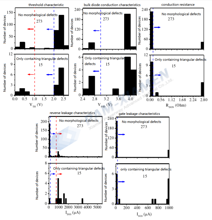
Fig. 4 Histograms of various characteristic distributions of SiC MOSFETs with triangle defects
| Table 1 Statistical table of the correlation between triangle defects and SiC MOSFET device characteristics | |||||
| Device characteristic | VTH degradation rate | VFSD degradation rate | RDON degradation rate | IDSS degradation rate | ISGS degradation rate |
| Triangle defect | 26% | 33% | 33% | 93% | 60% |
Overall, the study showed that the triangle defects have a significant impact on the failure and characteristic degradation of SiC MOSFET devices. The existence of triangle defects is the most fatal, with a failure rate of up to 93%, mainly manifested as a significant increase in reverse leakage of the device.

For more information, please contact us email at victorchan@powerwaywafer.com and powerwaymaterial@gmail.com.