The wafer of graphene for sale from PAM-XIAMEN are Monolayer Graphene on PET film, Monolayer Graphene on SiO2/Silicon, Bilayer Graphene on SiO2/Silicon, Monolayer Graphene on Copper, and graphene wafer growth on nickel for researches and industry.
Graphene is a new semiconductor material with a single-layer two-dimensional honeycomb lattice structure piled up by carbon atoms, which is connected by sp² hybridization. Graphene has excellent optical, electrical, and mechanical properties, which are equal to or exceed silicon performance. The frequency of processors made of graphene is 100 to 1000 times that of silicon chips. In the future, graphene wafers are expected to replace silicon wafers and become the next generation of semiconductor materials. The wafer scale graphene growth is usually by chemical vapor deposition (CVD).
1. Wafer List of Graphene Wafer
| Graphene Wafers/films | |
| Item No | Description |
| MG/PET-10-10 | Monolayer Graphene on PET film (10 mm x 10 mm) |
| MG/PET-20-20 | Monolayer Graphene on PET film(20 mm x 20 mm) |
| MG/PET-50-50 | Monolayer Graphene on PET film (50 mm x 50 mm) |
| MG/PET-100-100 | Monolayer Graphene on PET film (100 mm x 100 mm) |
| MG/PET-300-200 | Monolayer Graphene on PET film(300 mm x 200 mm) |
| MG/PET-500-200 | Monolayer Graphene on PET film (500 mm x 200 mm) |
| MG/SiO2/Si-10-10 | Monolayer Graphene on SiO2/Silicon (10mm x 10mm) |
| MG/SiO2/Si-25-25 | Monolayer Graphene on SiO2/Silicon(1 inch x 1 inch) |
| MG/SiO2/Si-100 | Monolayer Graphene on SiO2/Silicon (100mm Wafer) |
| BG/SiO2/Si-10-10 | Bilayer Graphene on SiO2/Silicon(10 mm x 10 mm) |
| TG/SiO2/Si-10-10 | Trilayer Graphene on SiO2/Silicon (10 mm x 10 mm) |
| MG/Cu-10-10 | Monolayer Graphene on Copper (10 mm x 10 mm) |
| MG/Cu-20-20 | Monolayer Graphene on Copper (20 mm x 20mm) |
| MG/Cu-25-25 | Monolayer Graphene on Copper (1 inch x 1 inch) |
| MG/Cu-50-50 | Monolayer Graphene on Cu (50 mm x 50 mm) |
| MG/Cu-100-50 | Monolayer Graphene on Cu (100 mm x 50 mm) |
| MG/Cu-100 | Monolayer Graphene on Cu (100mm wafers) |
| MG/Ni-10-10 | Graphene growth on nickel(10mm x 10mm) |
| MG/Ni-20-20 | Graphene growth on nickel(20mm x 20mm) |
| MG/Ni-30-20 | Graphene growth on nickel(30mm x 20mm) |
| MG/Ni-50-20 | Graphene growth on nickel(50mm x 20mm) |
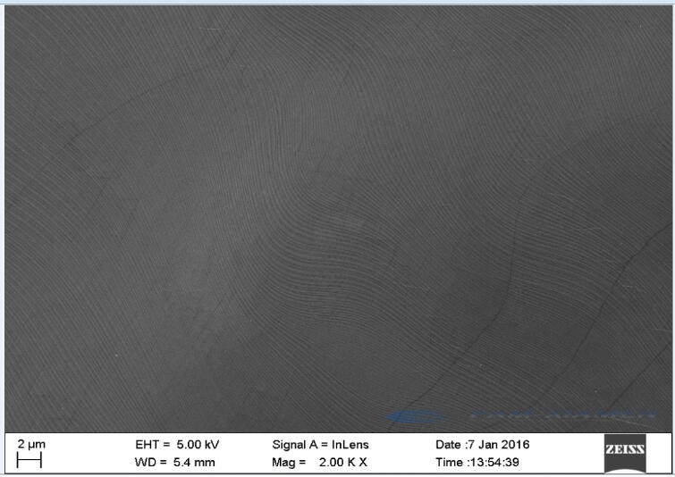
Below is a SEM or TEM image for monolayer graphene on copper foil, showing grain size and grain boundaries:
2. Graphene Properties
The carbon element composed of carbon atoms arranged neatly in a hexagonal lattice is graphene, which has a very stable structure. The connections among each carbon atoms of graphene are very pliable. When applying an external mechanical force, the carbon atom surface will bend and deform. The carbon atoms is no need to rearrange to fit the external force. So such a characteristic ensures the stability of the graphene structure, making graphene harder than diamond, and can be stretched like rubber. The stable lattice structure leads to an excellent electrical conductivity for graphene.

Graphene Substrate Structure
Because of the very strong force between the atoms, at room temperature, even if the surrounding carbon atoms collide, the electrons in graphene will suffer very little interference.
The electrons will not be scattered because of the lattice defects or the atoms introduced when the graphene electrons move in the orbit. The force between its atoms is very strong so that the electrons in graphene will face small interference even the surrounding atoms squeeze with each other.
Another characteristic of graphene is that its conductive electrons can move without obstacles in the lattice with a very fast speed, which far exceeds the moving speed of electrons in metal conductors or semiconductors. The thermal conductivity exceeds all existing known substances.
Graphene has very unique optical properties. Although there is only one layer of atoms, it can absorb 2.3% of the incident light in the entire wavelength range from visible light to infrared. The absorbed light will cause the generation of carriers (electrons and holes). The generation and transport of carriers in graphene are very different from traditional semiconductors.
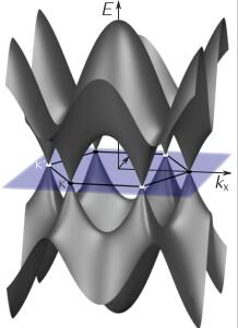
Graphene Electronic Band Structure
3. Graphene Wafer Prepared by CVD
CVD is the most commonly used technique for preparing single-layer graphene. The technology is the epitaxial growth of single-layer and multi-layer graphene by chemical vapor deposition of thermally decomposed hydrocarbons on a metal substrate. Use methane and other carbon-containing compounds as the carbon source (although methane is a standard reactant, but any carbon source can be used) through the high temperature decomposition and deposition of the carbon source on the surface of the substrate to achieve the growth of graphene (the copper foil is heated to 800-1000°C in a furnace). It is common to continuously produce graphene on copper foil. Chemical treatment can remove copper and deposit graphene on more useful substrates, such as SiO2. This method is simple and easy to implement, and progresses rapidly. It is currently the most widely used graphene preparation technology in industry, and the quality of the prepared graphene is relatively high.
Transparent graphene films are made by depositing carbon atoms on copper and etching away the copper. These films can be used for transparent conductive coating applications (such as touch screens).
Researchers use carbon diffusion through a layer of nickel to directly synthesize double-layer graphene directly on a SiO2 substrate without wafer graphene transfer. During the annealing process at 1000°C, the carbon source on top of the nickel decomposes and diffuses into the nickel layer. When cooled to room temperature, a double bilayer graphene is formed between the nickel layer and the SiO2 substrate. The nickel is etched away, leaving a layer of graphene directly coated on the silicon oxide, eliminating any transfer process. The obtained high-quality bilayer graphene coverage is about 70%. But the growth process takes place at 1000°C.
Bilayer graphene wafer is grown from a solid carbon source. This process only needs a temperature higher than room temperature (25-160°C) to directly synthesize graphene films on SiO2. The substrate can be silicon, or even plastic and glass. Micron-level particles are displayed on the surface of SiO2 Crystal grains, showing nano-scale crystal grains on the surface of plastic and glass. The ability to synthesize graphene directly on non-conductive substrates at low temperatures makes new possibilities for manufacturing multiple nanoelectronic devices.
4. Applications of Graphene Wafers
Graphene has excellent light transmittance (single layer ~97.7%), low density (area density of only 0.77 mg/m2), good properties, almost completely transparent but very dense. These excellent characteristics make graphene wafer bonding have great application potential and revolutionary changes in many fields such as graphene solar panels, electronic information, new materials, new energy, biomedicine, and environmental protection.
4.1 Gas sensor on Graphene Film
Graphene’s unique two-dimensional structure and huge surface area make it very sensitive to the surrounding environment. Even the adsorption or release of a gas molecule can be detected. The reason for achieving such sensitivity is that graphene is a material with extremely low electronic noise. Micron-scale sensors made of graphene substrate can detect individual events when gas molecules attach or detach from the graphene surface.
4.2 Integrated Circuits on Graphene Coated Silicon Wafer
The effective mass of electrons in wafer-scale graphene films is almost zero. Under normal circumstances, this phenomenon only occurs for special particles or in the case of relativity with high energy. In a condensed matter system, it shows that the electron mobility in graphene is very large, and the speed of electron movement exceeds that in other materials, and only very little heat is generated. Therefore, there is a huge potential for graphene on silicon wafer in the field of electronics.
Graphene has high carrier mobility and low noise. It has a high carrier mobility (approximately 10 am/V·s) 10 times that of commercial silicon wafers, and is not affected by temperature and doping effects. So graphene layer can be used as the channel in the field effect transistor.
4.3 Other Electronic Devices on Graphene Wafer
Transparent conductive film is an important part of touch devices and liquid crystal displays. The transparent and conductive properties of graphene can be used as a good material for transparent conductive films. Curved graphene wafer is often used as electrodes for solar cells, or as electronic components for touch screens, transparent heaters, handwriting boards, light-emitting devices, etc..

For more information, please contact us email at victorchan@powerwaywafer.com and powerwaymaterial@gmail.com.