FZ grown high-resistance silicon wafer is offered by PAM-XIAMEN for the fabrication of MEMS (Micro-electro Mechanical System). Silicon wafer is the common material for manufacturing integrated circuits in consumer electronics. Due to the availability and competitive price with high quality of silicon material, it is very attractive for MEMS applications. More parameters of silicon MEMS wafer please see table below:
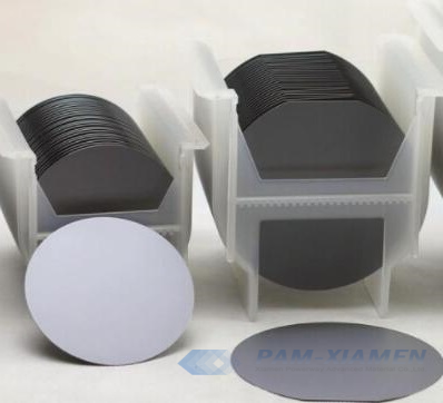
MEMS Wafer
1. Specification of MEMS Wafer
PAMP21445-SI
| Item | 4” Si HRS Wafer |
| Growth Method | FZ |
| Type | Intrinsic / Undoped |
| Thickness | 525 ± 25 μm |
| Orientation | <100> |
| Resistivity | >60000 ohm*cm |
| Surface Finished | DSP |
The diagram shows the radial resistance of MEMS silicon wafer:
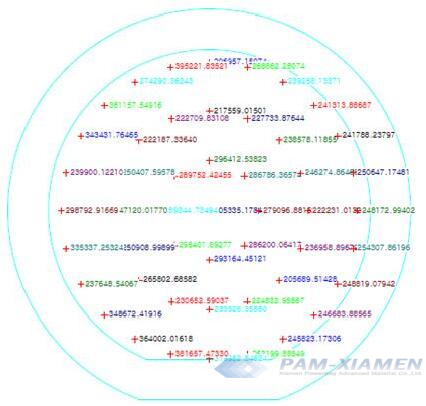
Radial Resistance Distribution of MEMS Wafer
Si MEMS wafer with a good resistivity tolerance grown by FZ has no oxygen, making it excellent for solar cell with high-efficient structure, RF MEMS device and photodiode. In addition, single crystal silicon has little energy dissipation. The MEMS wafer bonding technology will make the wafer bonding in MEMS, reducing the product size and weight, and increasing the convenience of MEMS-based product.
2. About Micro-Electro Mechanical System
MEMS is a micro device or system, which integrates interfaces communications, micro sensors, micro mechanical structures, micro actuators, micro power sources, signal processing and control circuits, and high-performance electronic integrated devices.
MEMS focuses on ultra-precision machining, involving in microelectronics, materials, mechanics, chemistry, mechanics and so on. Its disciplines cover the various branches of physics, chemistry, and mechanics such as force, electricity, light, magnetism, sound, and surface at the micro-scale.
Common types of MEMS products have MEMS accelerometer, MEMS microphone, MEMS gyroscope, MEMS pressure sensor, MEMS optical sensor, MEMS humidity sensor, MEMS gas sensors, micro motor, micro pump, micro vibrator, etc.
3. Silicon Wafer Stress in MEMS Applications
In MEMS applications, a single crystal silicon wafer is required to have a small stress. If the stress in the silicon single wafer is too large, the MEMS structure layer will be deformed or even broken, causing device failure. Therefore, for MEMS wafer fab, controlling the preparation process conditions of silicon high resistance wafers to make them have less stress has become a key issue in the MEMS manufacturing process.
To reduce the stress of silicon wafers for MEMS optical switches, we must start with the following aspects. In the silicon crystal drawing process, because the outside of the crystal cools faster than the inside, a large temperature gradient is generated in the radial direction of the crystal, and a large thermal stress is generated from this. Therefore, heat treatment technology must be used to reduce or eliminate the thermal stress of the crystal. . At the same time, the uneven doping concentration will also cause the internal stress of MEMS wafer. The radial uniformity of the resistivity must be controlled to achieve the purpose of reducing the thermal stress of the crystal. In addition, a certain mechanical stress will also be generated during the processing of silicon wafers. The mechanical stress of the silicon MEMS wafers can be reduced by optimizing the processing parameters.

For more information, please contact us email at victorchan@powerwaywafer.com and powerwaymaterial@gmail.com.