PAM-XIAMEN, a leading SiC epitaxial wafer manufacturer, can offer 4H SiC epitaxial wafers for MOS fabrication, which refer to a single crystal film(epitaxial layer) with certain requirements and the same crystal growing on a silicon carbide substrate. The SiC epitaxial wafer market size is 4 and 6 inch. In practical applications, the wide-bandgap semiconductor devices are almost made on the epitaxial layer, and the silicon carbide wafer itself only serves as the substrate, including the GaN epitaxial layer. Please refer to table below for more info about the SiC epi wafer.
1. Parameters of SiC Epitaxial Wafers
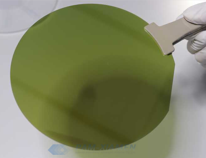
PAM-201218-SIC-EPI
| Size | 4 inch |
| Poly-type | 4H-SiC |
| Conductivity | N type |
| Diameter | 100mm |
| Thickness | 350um |
| Off-orientation toward | 4-degree off-axis |
| MPD | ≤1/cm2 |
| Resistivity | 0.015~0.028 ohm-cm |
| Surface finish | Double side polished |
| Buffer: | |
| Thickness | 0.5um, n type |
| doping level | 1E18cm3 |
| Epi 1: | |
| Thickness | 25um/50um |
| N-doping level | 1E15cm3 |
| Doping concentration | 1E15+/-20% |
| Uniformity | ≤10% |
| Thickness tolerance | +/-5% |
| Uniformity | ≤2% |
In fact, the parameters of the SiC epitaxial wafers mainly depend on the design of the device. For example, the parameters of the epitaxy are different according to the voltage level of the device.
Generally, the low voltage is 600 volts, the thickness of epitaxial growth in wafers we need may be about 6 μm; and the thickness of the medium voltage is 1200 to 1700, the thickness we need is 10 to 15 μm. If the high voltage is more than 10,000 volts, it may require more than 100 μm. Therefore, as the voltage capability increases, the epitaxial thickness increases. As a result, the preparation of high-quality silicon carbide epitaxial wafers is very difficult for epitaxial wafer suppliers, especially in the high-voltage field. The most important thing is the control of defects, which is actually a very big challenge in the SiC epitaxial wafer process.
2. Types Silicon Carbide Epitaxial Wafers Based on Usages
Silicon carbide is a typical representative of the third generation semiconductor materials. According to different usages, it can be divided into jewelry-grade silicon carbide materials, N-type SiC epitaxial wafers for power electronic devices, and semi-insulating silicon carbide materials for power radio frequency devices. Although the market for jewelry-grade silicon carbide materials and semi-insulating silicon carbide materials has grown rapidly in recent years, N-type SiC epi wafers play a main role in the future epitaxial wafer market.
For more information about SiC epitaxial wafers, please refer to:
What is the Key Parameters of SiC Epitaxial Wafer?
Why do We Need Silicon Carbide Epitaxial Wafer?
SiC-On-SiC Epi Wafer For Pin-Diodes
150mm 4H n-type SiC EPI wafers

For more information, please contact us email at victorchan@powerwaywafer.com and powerwaymaterial@gmail.com.