SiC wafer materials have broad bandgap, high electron saturation mobility, and excellent thermal properties, which have great application prospects in high-temperature, high-frequency, and high-power devices. The surface quality of Si surface directly affects the quality of SiC epitaxial thin film and the performance of its devices. However, defects on the C surface can increase the density of crystal dislocations, which can also lead to the formation of defects in the growth layer of the epitaxial thin film and affect device performance. Therefore, both the Si and C surfaces of SiC wafers require their surfaces to be ultra smooth, defect free, and undamaged.
PAM-XIAMEN can provide CMP processed Carbon (C) plane SiC wafers for device preparation researches, like MOS capacitor, specific parameters please contact our sales team: victorchan@powerwaywafer.com
1. Study on CMP Treatment of Si Surface and C Surfaceon SiC Substrate
K2S2Os were used as oxidants and Al2O3 nanoparticles as abrasives to compare the CMP polishing effects on the Si and C surfaces of 6H-SiC substrate. XPS was used to analyze the influence mechanism of different crystal faces on their CMP polishing effects. There is a significant difference in the CMP polishing effect between the Si and C surfaces of 6H-SiC wafers.
The material removal rate on the Si surface reaches a maximum value of 349nm/h at pH=6, while the material removal rate on the C surface reaches a maximum value of 1184 nm/h at pH=2. However, the polished Si and C faces are relatively smooth, with roughness values Ra of 0.58nm and 0.55nm, respectively.
After polishing, the XPS spectra of the Si and C surfaces are generally similar, but there are significant differences in the atomic composition between the Si and C surfaces. Fig. 1 shows that the concentration of O1s atoms and the ratio of C/Si and O/Si on the Si surface are higher than those on the C surface, but the concentration of C1s and Si2p atoms on the C surface is higher than that on the Si surface. Moreover, the C/Si ratio on both surfaces is higher than their normal stoichiometric ratio of 1. The peak intensity of Si-C binding energy on the C-plane is higher than that on the Si plane, but the content of oxidation products (such as Si4-C4-x-O2, Si4-C4-O4, C-O, and C=O) on the Si plane is higher than that on the C-plane, as shown in Fig.2. This indicates that the oxides on the C-plane are easier to remove than on the Si plane, so the C-plane is easier to obtain a higher material removal rate than on the Si plane.
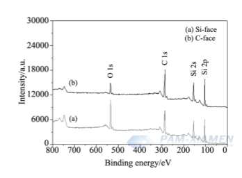
Fig. 1 XPS spectrum of polished surface of 6H-SiC wafer
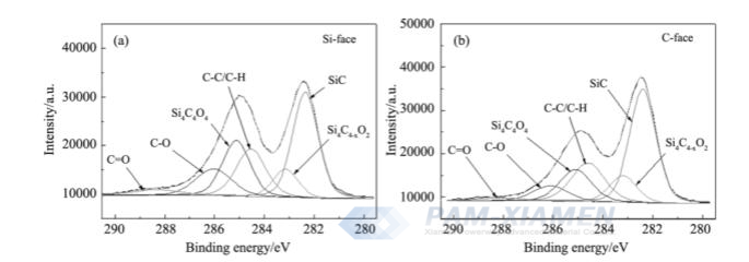
Fig. 2 C1s spectrum of polished surfaces of 6H-SiC (a) Si surface; (b) C-face
2. Study of MOS Capacitors on Si- and C -Face SiC Wafer
Scholars have studied the correlation between the atomic structure and electrical performance of corresponding SiC MOS capacitors, and discussed the intrinsic and extrinsic effects of interface structure and electrical defects on band offset modulation.
Obtained band structures of SiO2/SiC structures prepared under various conditions. The results indicate that the conduction band offset that determines the gate leakage current of SiC MOS devices and the resulting gate oxide reliability mainly depends on the substrate orientation and oxide thickness. Due to the smaller conduction band shift exhibited by the thin oxide on the C-surface substrate compared to the Si surface substrate, it concludes that the reduced reliability of SiC MOS devices manufactured on the C-face is an inherent issue, which may be due to the difference in electronegativity between Si and the C atoms bound to O atoms at the interface.
In addition, considering the accumulation of negative fixed charges at the SiO2/SiC interface, the increase in conduction band shift of thick oxides on Si and C substrates can be explained by the non intrinsic band modulation caused by interface defects.
From the perspective of reducing gate leakage, this expanded band offset of thick MOS devices is preferred, but electrical defects should have a negative impact on device performance and reliability. Therefore, basic strategies such as applying deposited gate oxides and utilizing stacked structures in band engineering are essential for utilizing MOS devices on C-face SiC.
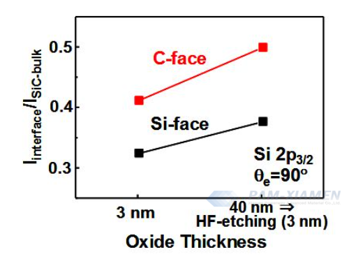
Fig. 3 Si 2p3/2 spectrum of changes in the total amount of intermediate oxide states from the oxide interface grown on SiC (0001) Si and C-faces
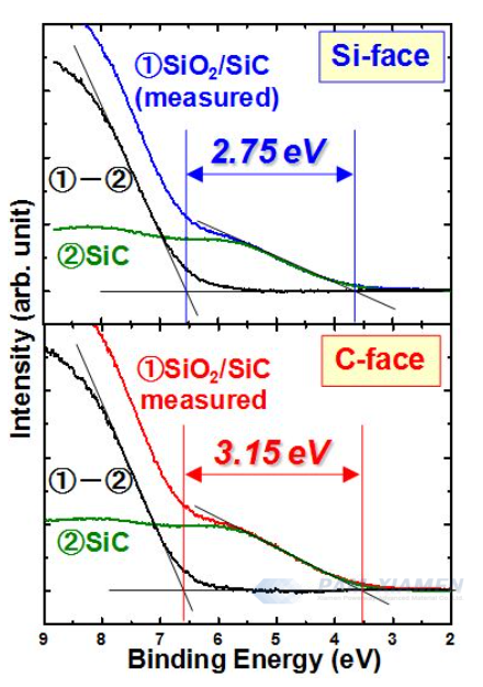
Fig. 4 Measurement and deconvolution valence band spectra of SiO2/SiC structures formed on Si and C faced 4H-SiC substrates, indicating that the valence band shift of SiO2/SiC on C-surface substrates is approximately 0.4 eV higher than that on Si surface.
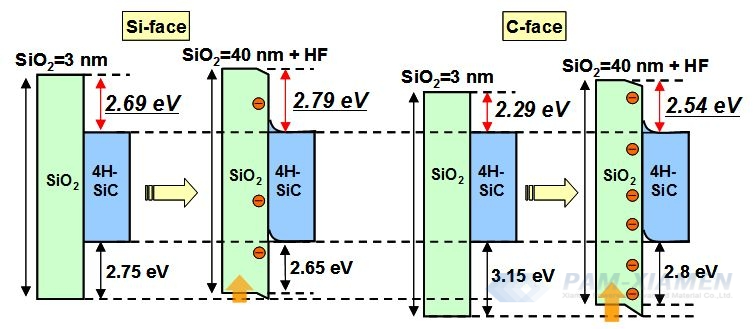
Fig. 5 Energy band diagram of SiO2/Si or C plane 4H-SiC structure by synchrotron XPS analysis. Measurement of valence band shift at SiO2/SiC interface formed under various conditions.
References:
1. CHEN Guo-mei, NI Zi-feng,QIAN Shan-hua , LIU Yuan-xiang,DU Chun-kuan, ZHOU Ling, XU Yi-e
en, ZHAO Yong-wu. Influence of Different Crystallographic Planes on CMP Performance of SiC Wafer
2. Heiji Watanabe, Takuji Hosoi. Fundamental Aspects of Silicon Carbide Oxidation

For more information, please contact us email at victorchan@powerwaywafer.com and powerwaymaterial@gmail.com.