The single crystal germanium is n type at room temperature, and the resistivity shows non-single dependence on temperature. When conduction type transits from n type to p type, the bulk germanium resistivity is in maximum, and the carrier mobility is declining. With the increasing of dopant concentration, the transition from inner to outer moves to room temperature and reflects the purity level of the crystal. Similar trend is found in high purity germanium single crystal doped with boron in different concentration. It is found that the interaction of temperature dependent and conductive principle caused by impurity band and intrinsic carrier in monocrystal germanium wafer results in the low receptor concentration (<1012/cm3). For extrinsic semiconductors, the resistance (conductivity) of the material is mainly related to the majority carrier concentration and mobility. The figure 1 shows the variation between resistivity and concentration of extrinsic germanium wafer:
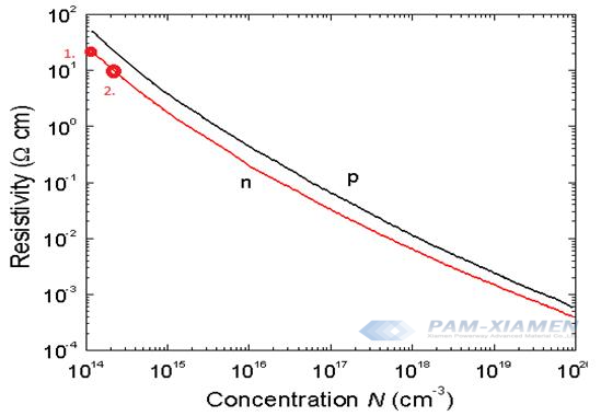
Fig. 1 Non-Linear Variation of P or N Type Germanium Resistivity and Concentration
In order to improve the yield rate at home and abroad, more stringent requirements have been put forward for the radial uniformity of resistivity of single crystal. Germanium single crystals are often affected by speed and solid-liquid interface during the production process. The germanium resistivity distribution is often uneven, and the uniformity of resistivity directly affects the reliability and yield of the device. The DC linear four-probe method of measuring resistivity plays a great role in the research and production of semiconductor materials, and is one of the most extensive testing methods.
1. DC Linear Four-Point Probe for Measuring the Resistance of Germanium Wafer
The DC linear four-probe applies to the measurement of the thickness of the sample and the closest distance from the edge of the sample to the end of any probe, both of which are greater than 4 times the resistivity of the probe pitch, and the measurement diameter is greater than 10 times the probe pitch. The resistivity of a single germanium wafer is less than 4 times the probe pitch. The measuring range is 1X10⁻³ohm.cm~1X10²ohm.cm.
2. Principle for Testing Extrinsic Resistivity of Germanium
The measurement principle is shown in Figure 2. The four probes arranged in a straight line are vertically pressed on the flat surface of the semi-infinite specimen. The current I (A) between the outer probes 1 and 4, and the voltage U (V) between the inner probes 2 and 3. Under certain conditions, the resistivity p of the sample near the four probes can be calculated by formula (1) and formula (2):
“l” is probe coefficient;
“l1” is the distance between probes 1 and 2, in centimeters (cm);
“l2” is the distance between probes 2, 3, in centimeters (cm);
“l3” is the distance between probes 3 and 4, in centimeters (cm).
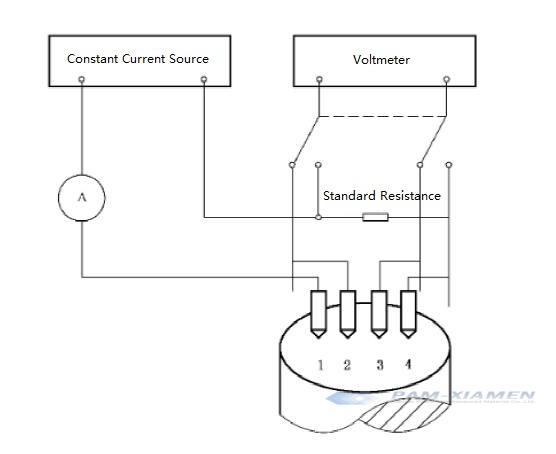
Fig. 2 Schematic Diagram of the Four-Probe Method
3. Equipment and Instruments for Determining Germanium Resistivity
Electromagnetic shielding room: In order to eliminate the parasitic current that the adjacent high-frequency generator may introduce in the measurement circuit, the germanium resistivity measurement must be carried out in an electromagnetic shielding room.
Constant temperature and humidity equipment: Ensure that the temperature in the resistivity test room can be stabilized within the arbitration temperature of 23±0.5°C, and the relative humidity is less than 70%.
Thermometer: Measure the surface temperature of germanium single crystal with accuracy within 0.1°C.
Four-probe resistivity tester includes:
Constant current power supply, which can provide 10-1A~10-5A DC current, its value is known and stable within ±0.5% during measurement;
Digital Voltmeter, which measures the voltage of 10-5V~1V, the error is less than ±0.5%. The input impedance of the meter should be more than three orders of magnitude greater than the resistance of the sample body plus the contact resistance between the sample and the probe;
Probe device:The probe head is made of tool steel, tungsten carbide and other materials. The diameter is about 0.5mm or 0.8mm. The indentation of the probe tip must be less than 100um. The probe spacing is measured with a measuring microscope (scale 0.01mm>. The mechanical movement rate between the probes △l/l<0.3% (△l is the maximum mechanical movement of the probe spacing, l is the probe spacing). The insulation resistance between probes is greater than 103 MΩ;
Probe holder, which is required to provide 5N~16N (total force), and it can ensure that the contact position of the probe and the sample is repeatedly within ±0.5% of the probe pitch.
4. Steps for Testing Resistivity of Germanium at Room Temperature
Step 1. Measurement environment: The sample is placed in a test room with a temperature of 23±0.5°C and a relative humidity of less than or equal to 70%.
Step 2. Sample preparation: The upper and lower surfaces of the sample to be tested are ground with W28# emery to ensure that there is no mechanical damage and no stains.
Step 3. Depending on the diameter of the single crystal, the following two measurement positions can be used:
* When the single crystal diameter is less than 100mm, the measurement position of the single crystal end surface resistivity is shown in Figure 3.

Fig. 3 Position for Measuring Resistivity of Pure Germanium under Standard Conditions, d <100mm
* When single crystal diameter is ≥100 mm, the measurement position of single crystal end face resistivity is shown in Figure 4.
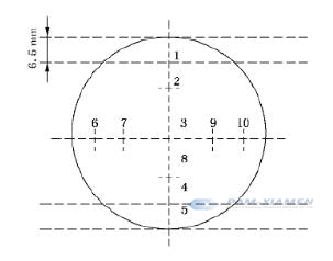
Fig. 4 Position for Measuring Germanium Resistivity under Standard Conditions, d ≥100mm
Step 4. Measurement: When the Ge sample reaches the specified temperature (23±0.5°C), press the probe vertically on the single model area cut flat on the sample table, and adjust the current to the specified value. The current should meet the weak field conditions: less than 1A/cm. The germanium rod current is selected according to Table 1. Take the average value of the voltage in the forward and reverse current directions. Calculate with different formulas according to the length of the sample, see Table 1.
Table 1 Current Selection Germanium Substrate with Different Resistivity
| Resistivity Range/(ohm*cm) | <0.01 | 0.01-1 | 1-30 | 30-100 |
| Current/mA | <100 | <10 | <1 | <0.1 |
| Recommended Wafer Current Value/mA | 100 | 2.5 | 0.25 | 0.025 |
5. Calculation of Resistivity of Germanium in ohm*cm
The thickness of the Ge wafer is greater than 4 times the probe pitch, and the single crystal section resistivity is calculated according to formula (1).
Calculation of single crystal radial resistivity variation:
* When the single crystal diameter is less than 100mm, the single crystal radial resistivity varies E uniformly, calculated according to formula (3).
E = [(pa – pc) / pc] * 100% ……(3)
In formula:
“pa” stands for the average value of germanium resistivity measured at 6mm from the edge, in ohm*cm;
“pc” represents the average value of the two resistivity measurements at the center, in ohm*cm.
* When the single crystal diameter>100mm, the maximum percentage change E of the Germanium single crystal radial resistivity is calculated according to formula (4).
E = [(pM – pm) / pm] * 100% ……(4)
In formula:
“pM” is the measured maximum resistivity, in ohm*cm;
“pm” is The measured minimum resistivity, in ohm*cm.
If the sample is a Ge wafer, calculate the geometric correction factor F:
Calculate the ratio of the sample thickness W to the average probe distance S, and use linear interpolation to find the correction factor F(W/S) from Table 2.
Table 2 Thickness correction factor F(W/S) is a function of the ratio of germanium wafer thickness W to probe spacing S:
| W/S | F(W/S) | W/S | F(W/S) | W/S | F(W/S) | W/S | F(W/S) |
| 0.1 | 1.0027 | 0.64 | 0.9885 | 0.91 | 0.9438 | 2.8 | 0.477 |
| 0.2 | 1.0007 | 0.65 | 0.9875 | 0.92 | 0.9414 | 2.9 | 0.462 |
| 0.3 | 1.0003 | 0.G6 | 0.9865 | 0.93 | 0.9391 | 3.0 | 0.448 |
| 0.4 | 0.9993 | 0.67 | 0.9853 | 0.94 | 0.9367 | 3.1 | 0.435 |
| 0.41 | 0.9992 | 0.68 | 0.9842 | 0.95 | 0.9343 | 3.2 | 0.422 |
| 0.42 | 0.9990 | 0.69 | 0.9830 | 0.96 | 0.9318 | 3.3 | 0.411 |
| 0.43 | 0.9989 | 0.70 | 0.9818 | 0.97 | 0.9293 | 3.4 | 0.399 |
| 0.44 | 0.9987 | 0.71 | 0.9804 | 0.98 | 0.9263 | 3.5 | 0.388 |
| 0.45 | 0.9986 | 0.72 | 0.9791 | 0.99 | 0.9242 | 3.6 | 0.378 |
| 0.46 | 0.9984 | 0.73 | 0.9777 | 1.0 | 0.921 | 3.7 | 0.369 |
| 0.47 | 0.9981 | 0.74 | 0.9762 | 1.1 | 0.894 | 3.8 | 0.359 |
| 0.48 | 0.9978 | 0.75 | 0.9747 | 1.2 | 0.864 | 3.9 | 0.350 |
| 0.49 | 0.9976 | 0.76 | 0.9731 | 1.3 | 0.834 | 4.0 | 0.342 |
| 0.50 | 0.9975 | 0.77 | 0.9715 | 1.4 | 0.803 | ||
| 0.51 | 0.9971 | 0.78 | 0.9699 | 1.5 | 0.772 | ||
| 0.52 | 0.9967 | 0.79 | 0.9681 | 1.6 | 0.742 | ||
| 0.53 | 0.9962 | 0.80 | 0.9664 | 1.7 | 0.713 | ||
| 0.54 | 0.9928 | 0.81 | 0.9645 | 1.8 | 0.685 | ||
| 0.55 | 0.9953 | 0.82 | 0.9627 | 1.9 | 0.659 | ||
| 0.56 | 0.9947 | 0.83 | 0.9608 | 2.0 | 0.634 | ||
| 0.57 | 0.9941 | 0.84 | 0.9588 | 2.1 | 0.601 | ||
| 0.58 | 0.9934 | 0.85 | 0.9566 | 2.2 | 0.587 | ||
| 0.59 | 0.9927 | 0.86 | 0.9547 | 2.3 | 0.566 | ||
| 0.60 | 0.9920 | 0.87 | 0.9526 | 2.4 | 0.546 | ||
| 0.61 | 0.9912 | 0.88 | 0.9505 | 2.5 | 0.528 | ||
| 0.62 | 0.9903 | 0.89 | 0.9483 | 2.6 | 0.510 | ||
| 0.63 | 0.9894 | 0.90 | 0.9460 | 2.7 | 0.493 |
Calculate the ratio of the average probe distance S to the sample diameter D, and find the correction factor F2
When 2.5≤W/S<4, F2 takes 4.532.
When 1<W/S<2.5, use linear interpolation to find F2 from Table 3.
Table 3 The correction factor F2 is a function of the ratio of the probe spacing S to the diameter D of the Ge wafer
| S/D | F2 | S/D | F2 | S/D | F2 |
| 0 | 4.532 | 0.035 | 4.485 | 0.070 | 4.348 |
| 0.005 | 4.531 | 0.040 | 4.470 | 0.075 | 4.322 |
| 0.010 | 4.528 | 0.045 | 4.454 | 0.080 | 4.294 |
| 0.015 | 4.524 | 0.050 | 4.436 | 0.085 | 4.265 |
| 0.020 | 4.517 | 0.055 | 4.417 | 0.090 | 4.235 |
| 0.025 | 4.508 | 0.060 | 4.395 | 0.095 | 4.204 |
| 0.030 | 4.497 | 0.065 | 4.372 | 0.100 | 4.171 |
Calculate the geometric correction factor F:
F=F(W / S) x W x F2 x Fsp……(5)
In formula:
“Fsp” is probe spacing correction factor;
“W” is sample thickness, in centimeters (cm).
Note: When W/S>1 and D>16S, the effective accuracy of F is within 2%.
6. Precision of the Germanium Resistance Measured
The repeatability of this standard for measuring the resistivity of germanium single crystal is better than ±10%;
The reproducibility of this standard for measuring the germanium resistivity is better than ±10%.

For more information, please contact us email at victorchan@powerwaywafer.com and powerwaymaterial@gmail.com.